MCP6V01/2/3 300 µA, Auto-Zeroed Op Amps Features Description • High DC Precision: - VOS Drift: ±50 nV/°C (maximum) - VOS: ±2 µV (maximum) - AOL: 130 dB (minimum) - PSRR: 130 dB (minimum) - CMRR: 130 dB (minimum) - Eni: 2.5 µVP-P (typical), f = 0.1 Hz to 10 Hz - Eni: 0.79 µVp-p (typical), f = 0.01 Hz to 1 Hz • Low Power and Supply Voltages: - IQ: 300 µA/amplifier (typical) - Wide Supply Voltage Range: 1.8V to 5.5V • Easy to Use: - Rail-to-Rail Input/Output - Gain Bandwidth Product: 1.
MCP6V01/2/3 Typical Application Circuit VIN R1 R2 R2 VDD/2 R3 VOUT C2 3 kΩ MCP6XXX MCP6V01 Offset Voltage Correction for Power Driver DS22058C-page 2 © 2008 Microchip Technology Inc.
MCP6V01/2/3 1.0 ELECTRICAL CHARACTERISTICS 1.1 Absolute Maximum Ratings † † Notice: Stresses above those listed under “Absolute Maximum Ratings” may cause permanent damage to the device. This is a stress rating only and functional operation of the device at those or any other conditions above those indicated in the operational listings of this specification is not implied. Exposure to maximum rating conditions for extended periods may affect device reliability. VDD – VSS ................................
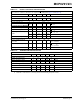
MCP6V01/2/3 TABLE 1-1: DC ELECTRICAL SPECIFICATIONS (CONTINUED) Electrical Characteristics: Unless otherwise indicated, TA = +25°C, VDD = +1.8V to +5.5V, VSS = GND, VCM = VDD/3, VOUT = VDD/2, VL = VDD/2, RL = 20 kΩ to VL, and CS = GND (refer to Figure 1-5 and Figure 1-6). Parameters Sym Min Typ Max Units Conditions VOL, VOH ISC VSS + 15 — VDD − 15 mV G = +2, 0.5V input overdrive — ±7 — mA VDD = 1.8V ISC — ±22 — mA VDD = 5.
MCP6V01/2/3 TABLE 1-3: DIGITAL ELECTRICAL SPECIFICATIONS Electrical Characteristics: Unless otherwise indicated, TA = +25°C, VDD = +1.8V to +5.5V, VSS = GND, VCM = VDD/3, VOUT = VDD/2, VL = VDD/2, RL = 20 kΩ to VL, CL = 60 pF, and CS = GND (refer to Figure 1-5 and Figure 1-6). Parameters Sym Min Typ Max Units Conditions RPD 3 5 — MΩ CS Logic Threshold, Low VIL VSS — 0.3VDD V CS Input Current, Low ICSL — 5 — pA CS Logic Threshold, High VIH 0.
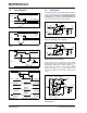
MCP6V01/2/3 1.3 Timing Diagrams 1.4 1.8V to 5.5V 1.8V VDD 0V tSTR VOS + 50 µV VOS Test Circuits The circuits used for the DC and AC tests are shown in Figure 1-5 and Figure 1-6. Lay the bypass capacitors out as discussed in Section 4.3.8 “Supply Bypassing and Filtering”. RN is equal to the parallel combination of RF and RG to minimize bias current effects. VDD VOS – 50 µV VIN FIGURE 1-1: Amplifier Start Up.
MCP6V01/2/3 2.0 TYPICAL PERFORMANCE CURVES Note: The graphs and tables provided following this note are a statistical summary based on a limited number of samples and are provided for informational purposes only. The performance characteristics listed herein are not tested or guaranteed. In some graphs or tables, the data presented may be outside the specified operating range (e.g., outside specified power supply range) and therefore outside the warranted range.
MCP6V01/2/3 Note: Unless otherwise indicated, TA = +25°C, VDD = +1.8V to 5.5V, VSS = GND, VCM = VDD/3, VOUT = VDD/2, VL = VDD/2, RL = 20 kΩ to VL, CL = 60 pF, and CS = GND. -2 -3 6.0 5.5 5.0 4.5 4.0 3.5 3.0 2.5 2.0 1.5 1.0 0.5 0.0 -0.5 -4 VDD = 1.8V 1/AOL (µV/V) Input Common Mode Voltage (V) FIGURE 2-11: 160 39 Samples TA = +25°C Soldered on PCB VDD = 5.5V 25% 20% 15% 10% VDD = 1.8V 5% DC Open-Loop Gain. VDD = 5.5V VDD = 1.
MCP6V01/2/3 Note: Unless otherwise indicated, TA = +25°C, VDD = +1.8V to 5.5V, VSS = GND, VCM = VDD/3, VOUT = VDD/2, VL = VDD/2, RL = 20 kΩ to VL, CL = 60 pF, and CS = GND. 1,000 Input Bias, Offset Currents (pA) DC Open-Loop Gain (dB) 160 155 VDD = 5.5V VDD = 1.8V 150 145 140 135 130 125 120 -25 0 25 50 75 Ambient Temperature (°C) 100 -IOS 10 125 IB 160 140 120 100 80 60 40 20 0 -20 -40 -60 IB 6.0 5.5 5.0 4.5 4.0 3.5 3.0 2.5 2.0 1.5 1.0 0.5 0.0 IOS -0.5 1.E-02 10m 1m 1.
MCP6V01/2/3 Note: Unless otherwise indicated, TA = +25°C, VDD = +1.8V to 5.5V, VSS = GND, VCM = VDD/3, VOUT = VDD/2, VL = VDD/2, RL = 20 kΩ to VL, CL = 60 pF, and CS = GND. Other DC Voltages and Currents 450 400 VDD = 5.5V Supply Current (µA) VDD = 1.8V VDD – VOH 300 250 200 100 50 VOL – VSS 125 FIGURE 2-20: Output Voltage Headroom vs. Ambient Temperature. DS22058C-page 10 6.5 6.0 5.5 5.0 4.5 4.0 3.5 3.0 2.5 2.0 15% 10% 5% 0% 1.7 100 20% 1.
MCP6V01/2/3 Note: Unless otherwise indicated, TA = +25°C, VDD = +1.8V to 5.5V, VSS = GND, VCM = VDD/3, VOUT = VDD/2, VL = VDD/2, RL = 20 kΩ to VL, CL = 60 pF, and CS = GND. POR Trip Voltage (V) 1.8 1.6 1.4 1.2 1.0 0.8 0.6 0.4 0.2 0.0 -50 -25 0 25 50 75 Ambient Temperature (°C) 100 125 FIGURE 2-24: Power On Reset Voltage vs. Ambient Temperature. © 2008 Microchip Technology Inc.
MCP6V01/2/3 Note: Unless otherwise indicated, TA = +25°C, VDD = +1.8V to 5.5V, VSS = GND, VCM = VDD/3, VOUT = VDD/2, VL = VDD/2, RL = 20 kΩ to VL, CL = 60 pF, and CS = GND. Frequency Response PSRR+ PSRR- 100 1.0 90 0.8 80 0.6 70 0.4 PM 0.2 CMRR and PSRR vs. VDD = 1.8V CL = 60 pF 30 -90 10 -150 | AOL | 0 -120 -180 -10 -210 -20 -240 10k 100k 1M 1.E+04 1.E+05 1.E+06 Frequency (Hz) -270 10M 1.E+07 VDD = 5.5V CL = 60 pF 50 0 -120 -150 -180 -210 -20 -240 -270 10M 1.
MCP6V01/2/3 Note: Unless otherwise indicated, TA = +25°C, VDD = +1.8V to 5.5V, VSS = GND, VCM = VDD/3, VOUT = VDD/2, 10k 1.E+04 100 VDD = 1.8V 1k 1.E+03 100 1.E+02 G = 1 V/V G = 10 V/V G = 100 V/V 10 1.E+01 1 1.E+00 100k 1.0E+05 1M 10M 1.0E+06 1.0E+07 Frequency (Hz) 50 40 VDD = 1.8V 30 20 1M 1.E+06 Frequency (Hz) 10M 1.E+07 FIGURE 2-33: Channel-to-Channel Separation vs. Frequency. Maximum Output Voltage Swing (V P-P ) Open-Loop Output Impedance ( Ω) VDD = 5.5V 60 10 1k 1.E+03 100 1.E+02 1.
MCP6V01/2/3 Note: Unless otherwise indicated, TA = +25°C, VDD = +1.8V to 5.5V, VSS = GND, VCM = VDD/3, VOUT = VDD/2, VL = VDD/2, RL = 20 kΩ to VL, CL = 60 pF, and CS = GND. Input Noise and Distortion 1000 VDD = 5.5V eni 100 100 VDD = 1.8V Eni(0 Hz to f) 10 10 1.E+01 10 100k 1.E+05 100 1k 10k 1.E+02 1.E+03 1.E+04 Frequency (Hz) FIGURE 2-35: vs. Frequency. 10 VDD = 5.5V VDD = 5.5V VDD = 1.8V 100 80 60 40 20 6.0 5.5 5.0 4.5 4.0 3.5 3.0 2.5 2.0 1.5 1.0 0.5 0.
MCP6V01/2/3 Note: Unless otherwise indicated, TA = +25°C, VDD = +1.8V to 5.5V, VSS = GND, VCM = VDD/3, VOUT = VDD/2, VL = VDD/2, RL = 20 kΩ to VL, CL = 60 pF, and CS = GND. Time Response VOS 20 40 60 0 4.5 4.0 VDD 4 3.5 2 3.0 0 2.5 -2 2.0 VOS -4 1.5 -6 1.0 -8 0.5 -10 Power Supply Voltage (V) 6 Input Offset Voltage (mV) 5.0 POR Trip Point 8 2 4 6 FIGURE 2-44: Step Response. FIGURE 2-41: Input Offset Voltage vs. Time with Temperature Change. 10 VDD = 5.
MCP6V01/2/3 Note: Unless otherwise indicated, TA = +25°C, VDD = +1.8V to 5.5V, VSS = GND, VCM = VDD/3, VOUT = VDD/2, VDD = 5.5V G = -1 Output Voltage (V) 5.0 5 10 FIGURE 2-47: Response. 15 20 25 30 Time (µs) 35 40 45 VOUT Inverting Large Signal Step VDD = 5.5V 0.8 Rising Edge 0.7 0.6 0.5 VDD = 1.8V 0.4 Falling Edge 0.2 0.1 0.0 -50 -25 FIGURE 2-48: Temperature. DS22058C-page 16 0 25 50 75 Ambient Temperature (°C) 100 Slew Rate vs. Ambient 125 5 4.0 4 3.0 3 2.0 2 1.
MCP6V01/2/3 Note: Unless otherwise indicated, TA = +25°C, VDD = +1.8V to 5.5V, VSS = GND, VCM = VDD/3, VOUT = VDD/2, VL = VDD/2, RL = 20 kΩ to VL, CL = 60 pF, and CS = GND. Chip Select Response (MCP6V03 only) 2.0 2.5 3.0 3.5 4.0 4.5 Power Supply Voltage (V) 5.0 5.5 Power Supply Current (µA) 350 300 Op Amp turns on here 250 Op Amp turns off here VDD = 1.8V G=1 VIN = 0.9V VL = 0V 200 150 Hysteresis 100 0.0 0.5 1.0 1.5 2.0 2.5 3.0 3.5 4.0 4.5 5.0 5.5 Chip Select Voltage (V) 50 0 0.2 0.4 0.
MCP6V01/2/3 Note: Unless otherwise indicated, TA = +25°C, VDD = +1.8V to 5.5V, VSS = GND, VCM = VDD/3, VOUT = VDD/2, VL = VDD/2, RL = 20 kΩ to VL, CL = 60 pF, and CS = GND. 7 65% VIH/VDD Pull-down Resistor (MΩ) VDD = 5.5V 60% 55% 50% 45% 40% 35% VIL/VDD VDD = 1.8V 4 3 2 1 FIGURE 2-58: 100 125 6.5 0 25 50 75 Ambient Temperature (°C) 6.0 -25 5.5 0.00 5.0 0.05 4.5 0.10 4.0 VDD = 1.8V 0.15 125 +125°C +85°C +25°C -40°C 3.5 0.20 100 CS = VDD Representative Part 3.0 VDD = 5.5V 0.
MCP6V01/2/3 3.0 PIN DESCRIPTIONS Descriptions of the pins are listed in Table 3-1.
MCP6V01/2/3 NOTES: DS22058C-page 20 © 2008 Microchip Technology Inc.
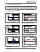
MCP6V01/2/3 4.0 APPLICATIONS 4.1 The MCP6V01/2/3 family of auto-zeroed op amps is manufactured using Microchip’s state of the art CMOS process. It is designed for low cost, low power and high precision applications. Its low supply voltage, low quiescent current and wide bandwidth makes the MCP6V01/2/3 ideal for battery-powered applications. Overview of Auto-zeroing Operation Figure 4-1 shows a simplified diagram of the MCP6V01/2/3 auto-zeroed op amps.
MCP6V01/2/3 4.1.2 AUTO-ZEROING ACTION Figure 4-2 shows the connections between amplifiers during the Normal Mode of operation (φ1). The hold capacitor (CH) corrects the Null Amplifier’s input offset. Since the Null Amplifier has very high gain, it dominates the signal seen by the Main Amplifier. This greatly reduces the impact of the Main Amplifier’s input offset voltage on overall performance.
MCP6V01/2/3 4.2 Other Functional Blocks 4.2.1 RAIL-TO-RAIL INPUTS The input stage of the MCP6V01/2/3 op amps uses two differential CMOS input stages in parallel. One operates at low common mode input voltage (VCM, which is approximately equal to VIN+ and VIN– in normal operation) and the other at high VCM. With this topology, the input operates with VCM up to 0.2V past either supply rail at +25°C (see Figure 2-18). The input offset voltage (VOS) is measured at VCM = VSS – 0.2V and VDD + 0.
MCP6V01/2/3 4.3 Application Tips 4.3.1 4.3.4 INPUT OFFSET VOLTAGE OVER TEMPERATURE Table 1-1 gives both the linear and quadratic temperature coefficients (TC1 and TC2) of input offset voltage.
MCP6V01/2/3 After selecting RISO for your circuit, double check the resulting frequency response peaking and step response overshoot. Modify RISO's value until the response is reasonable. Bench evaluation and simulations with the MCP6V01 SPICE macro model (good for all of the MCP6V01/2/3 op amps) are helpful. 4.3.6 STABILIZING OUTPUT LOADS This family of auto-zeroed op amps has an output impedance (Figure 2-31 and Figure 2-32) that has a double zero when the gain is low.
MCP6V01/2/3 4.3.9 PCB DESIGN FOR DC PRECISION In order to achieve DC precision on the order of ±1 µV, many physical errors need to be minimized. The design of the Printed Circuit Board (PCB), the wiring, and the thermal environment has a strong impact on the precision achieved. A poor PCB design can easily be more than 100 times worse than the MCP6V01/2/3 op amps minimum and maximum specifications. 4.3.9.
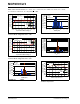
MCP6V01/2/3 4.3.9.3 Difference Amplifier Layout for Thermo-junctions Figure 4-12 shows the recommended difference amplifier circuit. Usually, we choose R1 = R2 and R3 = R4. The guard traces (with ground vias at the ends) help minimize the thermal gradients.
MCP6V01/2/3 4.3.9.5 Other PCB Thermal Design Tips In cases where an individual resistor needs to have its thermo-junction voltage cancelled, it can be split into two equal resistors as shown in Figure 4-14. To keep the thermal gradients near the resistors as small as possible, the layouts are symmetrical with a ring of metal around the outside. Make R1A = R1B = R1/2 and R2A = R2B = 2R2. R1A R1B R2A R2B R1A R1B R2A R2B FIGURE 4-14: Resistors.
MCP6V01/2/3 4.4 Typical Applications 4.4.1 4.4.2 WHEATSTONE BRIDGE Many sensors are configured as Wheatstone bridges. Strain gauges and pressure sensors are two common examples. These signals can be small and the common mode noise large. Amplifier designs with high differential gain are desirable. RTD SENSOR The ratiometric circuit in Figure 4-17 conditions a three wire RTD. It corrects for the sensor’s wiring resistance by subtracting the voltage across the middle RW.
MCP6V01/2/3 4.4.3 THERMOCOUPLE SENSOR Figure 4-18 shows a simplified diagram of an amplifier and temperature sensor used in a thermocouple application. The type K thermocouple senses the temperature at the hot junction (THJ), and produces a voltage at V1 proportional to THJ (in °C). The amplifier’s gain is is set so that V4/THJ is 10 mV/°C. V3 represents the output of a temperature sensor, which produces a voltage proportional to the temperature (in °C) at the cold junction (TCJ), and with a 0.50V offset.
MCP6V01/2/3 5.0 DESIGN AIDS Microchip provides the basic design aids needed for the MCP6V01/2/3 family of op amps. 5.1 SPICE Macro Model The latest SPICE macro model for the MCP6V01/2/3 op amps is available on the Microchip web site at www.microchip.com. This model is intended to be an initial design tool that works well in the op amp’s linear region of operation over the temperature range. See the model file for information on its capabilities.
MCP6V01/2/3 NOTES: DS22058C-page 32 © 2008 Microchip Technology Inc.
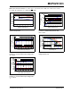
MCP6V01/2/3 6.0 PACKAGING INFORMATION 6.1 Package Marking Information Example 8-Lead DFN (4x4) (MCP6V02) XXXXXX XXXXXX YYWW NNN 6V02 e3 E/MD^^ 0750 256 Example: 8-Lead SOIC (150 mil) XXXXXXXX XXXXYYWW NNN MCP6VO1E SN e3 0750 256 Example: 8-Lead TDFN (2x3) (MCP6V01, MCP6V03) XXX YWW NN Device Code MCP6V01 AAA MCP6V03 AAB AAA 838 25 Note: Applies to 8-Lead 2x3 TDFN Legend: XX...
MCP6V01/2/3 /HDG 3ODVWLF 'XDO )ODW 1R /HDG 3DFNDJH 0' ± [ [ PP %RG\ >')1@ 1RWH )RU WKH PRVW FXUUHQW SDFNDJH GUDZLQJV SOHDVH VHH WKH 0LFURFKLS 3DFNDJLQJ 6SHFLILFDWLRQ ORFDWHG DW KWWS ZZZ PLFURFKLS FRP SDFNDJLQJ D e b N N L E E2 K EXPOSED PAD 1 2 2 1 NOTE 1 NOTE 1 D2 TOP VIEW BOTTOM VIEW A3 A A1 NOTE 2 8QLWV 'LPHQVLRQ /LPLWV 1XPEHU RI 3LQV 0,//,0(7(56 0,1 1 120 0$; 3LWFK H 2YHUDOO +HLJKW $ 6WDQGRII $ &RQWDFW 7KLFNQHVV $ 2YHU
MCP6V01/2/3 /HDG 3ODVWLF 6PDOO 2XWOLQH 61 ± 1DUURZ PP %RG\ >62,&@ 1RWH )RU WKH PRVW FXUUHQW SDFNDJH GUDZLQJV SOHDVH VHH WKH 0LFURFKLS 3DFNDJLQJ 6SHFLILFDWLRQ ORFDWHG DW KWWS ZZZ PLFURFKLS FRP SDFNDJLQJ D e N E E1 NOTE 1 1 2 3 α h b h A2 A c φ L A1 L1 8QLWV 'LPHQVLRQ /LPLWV 1XPEHU RI 3LQV β 0,//,0(7(56 0,1 1 120 0$; 3LWFK H 2YHUDOO +HLJKW $ ± %6& ± 0ROGHG 3DFNDJH 7KLFNQHVV $ ± ± 6WDQGRII $ ± 2YHUDOO :LGWK ( 0ROGHG 3DFNDJH :LGWK
MCP6V01/2/3 /HDG 3ODVWLF 6PDOO 2XWOLQH 61 ± 1DUURZ PP %RG\ >62,&@ 1RWH )RU WKH PRVW FXUUHQW SDFNDJH GUDZLQJV SOHDVH VHH WKH 0LFURFKLS 3DFNDJLQJ 6SHFLILFDWLRQ ORFDWHG DW KWWS ZZZ PLFURFKLS FRP SDFNDJLQJ DS22058C-page 36 © 2008 Microchip Technology Inc.
MCP6V01/2/3 /HDG 3ODVWLF 'XDO )ODW 1R /HDG 3DFNDJH 01 ± [ [ PP %RG\ >7')1@ 1RWH )RU WKH PRVW FXUUHQW SDFNDJH GUDZLQJV SOHDVH VHH WKH 0LFURFKLS 3DFNDJLQJ 6SHFLILFDWLRQ ORFDWHG DW KWWS ZZZ PLFURFKLS FRP SDFNDJLQJ © 2008 Microchip Technology Inc.
MCP6V01/2/3 /HDG 3ODVWLF 'XDO )ODW 1R /HDG 3DFNDJH 01 ± [ [ PP %RG\ >7')1@ 1RWH )RU WKH PRVW FXUUHQW SDFNDJH GUDZLQJV SOHDVH VHH WKH 0LFURFKLS 3DFNDJLQJ 6SHFLILFDWLRQ ORFDWHG DW KWWS ZZZ PLFURFKLS FRP SDFNDJLQJ DS22058C-page 38 © 2008 Microchip Technology Inc.
MCP6V01/2/3 APPENDIX A: REVISION HISTORY Revision C (December 2008) The following is the list of modifications: 1. 2. 3. 4. 5. 6. Added the 8-lead, 2x3 TDFN package for the MCP6V01 and MCP6V03 devices. Corrected the IMD specification in Table 1-2. Added 8-lead, 2x3 TDFN package information to Thermal Characteristic table. Added information on the Exposed Thermal Pad (EP) for the 8-lead, 2x3 TDFN and 8-lead, 4x4 DFN packages. Added Section 4.3.
MCP6V01/2/3 APPENDIX B: OFFSET RELATED TEST SCREENS We use production screens to ensure the quality of our outgoing products. These screens are set at wider limits to eliminate any fliers; see Table B-1. Input offset voltage related specifications in the DC spec table (Table 1-1) are based on bench measurements (see Section 2.1 “DC Input Precision”).
MCP6V01/2/3 PRODUCT IDENTIFICATION SYSTEM To order or obtain information, e.g., on pricing or delivery, refer to the factory or the listed sales office. PART NO.
MCP6V01/2/3 NOTES: DS22058C-page 44 © 2008 Microchip Technology Inc.
Note the following details of the code protection feature on Microchip devices: • Microchip products meet the specification contained in their particular Microchip Data Sheet. • Microchip believes that its family of products is one of the most secure families of its kind on the market today, when used in the intended manner and under normal conditions. • There are dishonest and possibly illegal methods used to breach the code protection feature.
WORLDWIDE SALES AND SERVICE AMERICAS ASIA/PACIFIC ASIA/PACIFIC EUROPE Corporate Office 2355 West Chandler Blvd. Chandler, AZ 85224-6199 Tel: 480-792-7200 Fax: 480-792-7277 Technical Support: http://support.microchip.com Web Address: www.microchip.