
Datasheet


© 2008 Microchip Technology Inc. DS22058C-page 3
MCP6V01/2/3
1.0 ELECTRICAL CHARACTERISTICS
1.1 Absolute Maximum Ratings †
V
DD
–V
SS
.......................................................................6.5V
Current at Input Pins ....................................................±2 mA
Analog Inputs (V
IN
+ and V
IN
–) †† ... V
SS
– 1.0V to V
DD
+1.0V
All other Inputs and Outputs ............ V
SS
– 0.3V to V
DD
+0.3V
Difference Input voltage ...................................... |V
DD
–V
SS
|
Output Short Circuit Current ................................ Continuous
Current at Output and Supply Pins ............................±30 mA
Storage Temperature ...................................-65°C to +150°C
Max. Junction Temperature ........................................ +150°C
ESD protection on all pins (HBM, MM) ................≥ 4 kV, 300V
† Notice: Stresses above those listed under “Absolute
Maximum Ratings” may cause permanent damage to the
device. This is a stress rating only and functional operation of
the device at those or any other conditions above those
indicated in the operational listings of this specification is not
implied. Exposure to maximum rating conditions for extended
periods may affect device reliability.
†† See Section 4.2.1 “Rail-to-Rail Inputs”.
1.2 Specifications
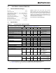
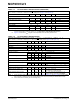
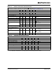
TABLE 1-1: DC ELECTRICAL SPECIFICATIONS
Electrical Characteristics: Unless otherwise indicated, T
A
= +25°C, V
DD
= +1.8V to +5.5V, V
SS
= GND, V
CM
= V
DD
/3,
V
OUT
=V
DD
/2, V
L
=V
DD
/2, R
L
= 20 kΩ to V
L
, and CS = GND (refer to Figure 1-5 and Figure 1-6).
Parameters Sym Min Typ Max Units Conditions
Input Offset
Input Offset Voltage V
OS
-2.0 — +2.0 µV T
A
= +25°C (Note 1)
Input Offset Voltage Drift with Temperature
(linear Temp. Co.)
TC
1
-50 — +50 nV/°C T
A
= -40 to +125°C
(Note 1)
Input Offset Voltage Quadratic Temp. Co. TC
2
—±0.1—nV/°C
2
T
A
= -40 to +125°C
Power Supply Rejection PSRR 130 143 — dB (Note 1)
Input Bias Current and Impedance
Input Bias Current I
B
—±1—pA
Input Bias Current across Temperature I
B
—60—pAT
A
= +85°C
I
B
— 600 5000 pA T
A
= +125°C
Input Offset Current I
OS
—-30— pA
Input Offset Current across Temperature I
OS
—-50— pAT
A
= +85°C
I
OS
-1000 -75 1000 pA T
A
= +125°C
Common Mode Input Impedance Z
CM
—10
13
||6 — Ω||pF
Differential Input Impedance Z
DIFF
—10
13
||6 — Ω||pF
Common Mode
Common-Mode Input Voltage Range V
CMR
V
SS
− 0.20 — V
DD
+0.20 V (Note 2)
Common-Mode Rejection CMRR 130 142 — dB V
DD
= 1.8V,
V
CM
= -0.2V to 2.0V
(Note 1, Note 2)
CMRR 140 152 — dB V
DD
= 5.5V,
V
CM
= -0.2V to 5.7V
(Note 1, Note 2)
Open-Loop Gain
DC Open-Loop Gain (large signal) A
OL
130 145 — dB V
DD
=1.8V,
V
OUT
= 0.2V to 1.6V (Note 1)
A
OL
140 156 — dB V
DD
=5.5V,
V
OUT
= 0.2V to 5.3V (Note 1)
Note 1: Set by design and characterization. Due to thermal junction and other effects in the production environment, these parts
can only be screened in production (except TC
1
; see Appendix B: “Offset Related Test Screens”).
2: Figure 2-18 shows how V
CMR
changed across temperature for the first three production lots.