
Datasheet


MCP6V01/2/3
DS22058C-page 4 © 2008 Microchip Technology Inc.
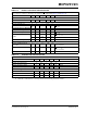
Output
Maximum Output Voltage Swing V
OL
, V
OH
V
SS
+15 — V
DD
− 15 mV G = +2, 0.5V input overdrive
Output Short Circuit Current I
SC
—±7—mAV
DD
=1.8V
I
SC
—±22— mAV
DD
=5.5V
Power Supply
Supply Voltage V
DD
1.8 — 5.5 V
Quiescent Current per amplifier I
Q
200 300 400 µA I
O
= 0
POR Trip Voltage V
POR
1.15 — 1.65 V
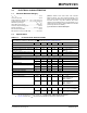
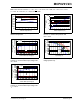
TABLE 1-1: DC ELECTRICAL SPECIFICATIONS (CONTINUED)
Electrical Characteristics: Unless otherwise indicated, T
A
= +25°C, V
DD
= +1.8V to +5.5V, V
SS
= GND, V
CM
= V
DD
/3,
V
OUT
=V
DD
/2, V
L
=V
DD
/2, R
L
= 20 kΩ to V
L
, and CS = GND (refer to Figure 1-5 and Figure 1-6).
Parameters Sym Min Typ Max Units Conditions
Note 1: Set by design and characterization. Due to thermal junction and other effects in the production environment, these parts
can only be screened in production (except TC
1
; see Appendix B: “Offset Related Test Screens”).
2: Figure 2-18 shows how V
CMR
changed across temperature for the first three production lots.
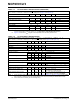
TABLE 1-2: AC ELECTRICAL SPECIFICATIONS
Electrical Characteristics: Unless otherwise indicated, T
A
= +25°C, V
DD
= +1.8V to +5.5V, V
SS
= GND, V
CM
= V
DD
/3,
V
OUT
=V
DD
/2, V
L
=V
DD
/2, R
L
= 20 kΩ to V
L
, C
L
= 60 pF, and CS = GND (refer to Figure 1-5 and Figure 1-6).
Parameters Sym Min Typ Max Units Conditions
Amplifier AC Response
Gain Bandwidth Product GBWP — 1.3 — MHz
Slew Rate SR — 0.5 — V/µs
Phase Margin PM — 65 — ° G = +1
Amplifier Noise Response
Input Noise Voltage E
ni
—0.79 — µV
P-P
f = 0.01 Hz to 1 Hz
E
ni
—2.5 —µV
P-P
f = 0.1 Hz to 10 Hz
Input Noise Voltage Density e
ni
—120 —nV/√Hz f < 2.5 kHz
e
ni
—45 —nV/√Hz f = 100 kHz
Input Noise Current Density i
ni
—0.6 —fA/√Hz
Amplifier Distortion (Note 1)
Intermodulation Distortion (AC) IMD — <1 — µV
PK
V
CM
tone = 50 mV
PK
at 1 kHz, G
N
= 1, V
DD
= 1.8V
IMD — <1 — µV
PK
V
CM
tone = 50 mV
PK
at 1 kHz, G
N
= 1, V
DD
= 5.5V
Amplifier Step Response
Start Up Time t
STR
—500 — µs V
OS
within 50 µV of its final value
Offset Correction Settling Time t
STL
— 300 — µs G = +1, V
IN
step of 2V,
V
OS
within 50 µV of its final value
Output Overdrive Recovery Time t
ODR
— 100 — µs G = -100, ±0.5V input overdrive to V
DD
/2,
V
IN
50% point to V
OUT
90% point (Note 2)
Note 1: These parameters were characterized using the circuit in Figure 1-7. Figure 2-37 and Figure 2-38 show both an IMD
tone at DC and a residual tone at1 kHz; all other IMD and clock tones are spread by the randomization circuitry.
2: t
ODR
includes some uncertainty due to clock edge timing.