
Datasheet


© 2008 Microchip Technology Inc. DS22058C-page 7
MCP6V01/2/3
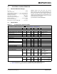
2.0 TYPICAL PERFORMANCE CURVES
Note: Unless otherwise indicated, T
A
= +25°C, V
DD
= +1.8V to 5.5V, V
SS
= GND, V
CM
=V
DD
/3, V
OUT
=V
DD
/2,
V
L
=V
DD
/2, R
L
=20kΩ to V
L
, C
L
= 60 pF, and CS = GND.
2.1 DC Input Precision
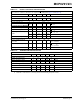
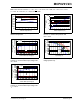
FIGURE 2-1: Input Offset Voltage.
FIGURE 2-2: Input Offset Voltage Drift.
FIGURE 2-3: Input Offset Voltage
Quadratic Temp Co.
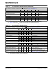
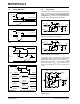
FIGURE 2-4: Input Offset Voltage vs.
Power Supply Voltage with V
CM
=V
CMR_L
.
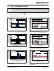
FIGURE 2-5: Input Offset Voltage vs.
Power Supply Voltage with V
CM
=V
CMR_H
.
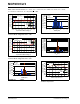
FIGURE 2-6: Input Offset Voltage vs.
Output Voltage.
Note: The graphs and tables provided following this note are a statistical summary based on a limited number of
samples and are provided for informational purposes only. The performance characteristics listed herein
are not tested or guaranteed. In some graphs or tables, the data presented may be outside the specified
operating range (e.g., outside specified power supply range) and therefore outside the warranted range.
0%
2%
4%
6%
8%
10%
12%
14%
16%
18%
20%
-1.5
-1.0
-0.5
0.0
0.5
1.0
1.5
Input Offset Voltage (µV)
Percentage of Occurrences
78 Samples
T
A
= +25°C
V
DD
= 1.8V and 5.5V
Soldered on PCB
0%
2%
4%
6%
8%
10%
12%
14%
16%
18%
20%
22%
-50
-40
-30
-20
-10
0
10
20
30
40
50
Input Offset Voltage Drift; TC
1
(nV/°C)
Percentage of Occurrences
78 Samples
V
DD
= 1.8V and 5.5V
Soldered on PCB
0%
2%
4%
6%
8%
10%
12%
14%
16%
18%
20%
22%
-0.4
-0.3
-0.2
-0.1
0.0
0.1
0.2
0.3
0.4
Input Offset Voltage's Quadratic Temp Co;
TC
2
(nV/°C
2
)
Percentage of Occurrences
78 Samples
V
DD
= 1.8V and 5.5V
Soldered on PCB
-4
-3
-2
-1
0
1
2
3
4
0.0 0.5 1.0 1.5 2.0 2.5 3.0 3.5 4.0 4.5 5.0 5.5 6.0 6.5
Power Supply Voltage (V)
Input Offset Voltage (µV)
+125°C
+85°C
+25°C
-40°C
V
CM
= V
CMR_L
Representative Part
-4
-3
-2
-1
0
1
2
3
4
0.0 0.5 1.0 1.5 2.0 2.5 3.0 3.5 4.0 4.5 5.0 5.5 6.0 6.5
Power Supply Voltage (V)
Input Offset Voltage (µV)
+125°C
+85°C
+25°C
-
40°C
V
CM
= V
CMR_H
Representative Part
-4
-3
-2
-1
0
1
2
3
4
0.00.51.01.52.02.53.03.54.04.55.05.5
Output Voltage (V)
Input Offset Voltage (µV)
V
DD
= 1.8V
V
DD
= 5.5V
Representative Part