
Datasheet


MCP6V01/2/3
DS22058C-page 8 © 2008 Microchip Technology Inc.
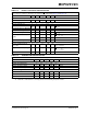
Note: Unless otherwise indicated, T
A
= +25°C, V
DD
= +1.8V to 5.5V, V
SS
= GND, V
CM
=V
DD
/3, V
OUT
=V
DD
/2,
V
L
=V
DD
/2, R
L
=20kΩ to V
L
, C
L
= 60 pF, and CS = GND.
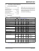
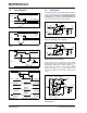
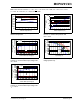
FIGURE 2-7: Input Offset Voltage vs.
Common Mode Voltage with V
DD
=1.8V.
FIGURE 2-8: Input Offset Voltage vs.
Common Mode Voltage with V
DD
=5.5V.
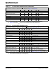
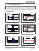
FIGURE 2-9: CMRR.
FIGURE 2-10: PSRR.
FIGURE 2-11: DC Open-Loop Gain.
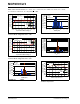
FIGURE 2-12: CMRR and PSRR vs.
Ambient Temperature.
-4
-3
-2
-1
0
1
2
3
4
-0.6
-0.4
-0.2
0.0
0.2
0.4
0.6
0.8
1.0
1.2
1.4
1.6
1.8
2.0
2.2
2.4
Input Common Mode Voltage (V)
Input Offset Voltage (µV)
V
DD
= 1.8V
Representative Part
+125°C
+85°C
+25°C
-40°C
-4
-3
-2
-1
0
1
2
3
4
-0.5
0.0
0.5
1.0
1.5
2.0
2.5
3.0
3.5
4.0
4.5
5.0
5.5
6.0
Input Common Mode Voltage (V)
Input Offset Voltage (µV)
V
DD
= 5.5V
Representative Part
+125°C
+85°C
+25°C
-40°C
0%
5%
10%
15%
20%
25%
30%
35%
-0.3
-0.2
-0.1
0.0
0.1
0.2
0.3
1/CMRR (µV/V)
Percentage of Occurrences
39 Samples
T
A
= +25°C
Soldered on PCB
V
DD
= 1.8V
V
DD
= 5.5V
0%
2%
4%
6%
8%
10%
12%
14%
-0.3
-0.2
-0.1
0.0
0.1
0.2
0.3
1/PSRR (µV/V)
Percentage of Occurrences
40 Samples
T
A
= +25°C
Soldered on PCB
0%
5%
10%
15%
20%
25%
30%
35%
40%
45%
50%
55%
-0.3
-0.2
-0.1
0.0
0.1
0.2
0.3
1/A
OL
(µV/V)
Percentage of Occurrences
40 Samples
T
A
= +25°C
V
DD
= 1.8V
V
DD
= 5.5V
120
125
130
135
140
145
150
155
160
-50 -25 0 25 50 75 100 125
Ambient Temperature (°C)
CMRR, PSRR (dB)
PSRR
CMRR
V
DD
= 5.5V
V
DD
= 1.8V