
User Guide

...........continued
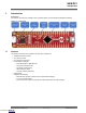
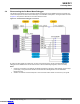
Debugger Signal ICSP Target Description
VTG - Target voltage
GND - Common ground.
DBG0 SWDATA Debug data line.
DBG3 nRESET Reset line
VOFF - Voltage Off input.
VBUS - VBUS voltage for external use.
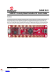
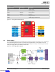
Figure 3-1. Curiosity Nano Standard Pinout
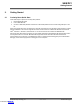
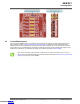
3.3 Power Supply
The evaluation kit is powered through the USB port and contains two regulators for generating 3.3V for the debugger
and an adjustable regulator for the target. The voltage from the USB connector can vary between 4.4V-5.25V
(according to the USB specification) and will limit the maximum voltage to the target. The following figure shows the
entire power supply system on the SAM D21 Curiosity Nano.
Figure 3-2. Power Supply Block Diagram
SAM D21
Curiosity Nano
© 2020 Microchip Technology Inc.
User Guide
DS70005409C-page 7
Downloaded from Arrow.com.Downloaded from Arrow.com.Downloaded from Arrow.com.Downloaded from Arrow.com.Downloaded from Arrow.com.Downloaded from Arrow.com.Downloaded from Arrow.com.