USB251xB/xBi USB 2.0 Hi-Speed Hub Controller General Description Features The Microchip USB251xB/xBi hub is a family of lowpower, configurable, MTT (multi transaction translator) hub controller IC products for embedded USB solutions. The x in the part number indicates the number of downstream ports available, while the B indicates battery charging support.
USB251xB/xBi TO OUR VALUED CUSTOMERS It is our intention to provide our valued customers with the best documentation possible to ensure successful use of your Microchip products. To this end, we will continue to improve our publications to better suit your needs. Our publications will be refined and enhanced as new volumes and updates are introduced. If you have any questions or comments regarding this publication, please contact the Marketing Communications Department via E-mail at docerrors@microchip.com.
USB251xB/xBi Table of Contents 1.0 Introduction ..................................................................................................................................................................................... 4 2.0 Block Diagram ................................................................................................................................................................................. 6 3.0 Pin Information ..............................................................
USB251xB/xBi 1.0 INTRODUCTION The Microchip USB251xB/xBi hub family is a group of low-power, configurable, MTT (multi transaction translator) hub controller ICs. The hub provides downstream ports for embedded USB solutions and is fully compliant with the USB 2.0 Specification [1]. Each of the hub controllers can attach to an upstream port as a full-speed or full-/hi-speed hub. The hub can support low-speed, full-speed, and hi-speed downstream devices when operating as a hi-speed hub.
USB251xB/xBi TABLE 1-1: SUMMARY OF COMPATIBILITIES BETWEEN USB251XB/XBI AND USB251X/XI/XA/XAI PRODUCTS Part Number Drop-in Replacement USB2512 USB2512B USB2512i USB2512Bi USB2512A USB2512B USB2512Ai USB2512Bi USB2513 USB2513B USB2513i USB2513Bi USB2514 USB2514B USB2514i USB2514Bi Conventions Within this manual, the following abbreviations and symbols are used to improve readability. Example BIT FIELD.
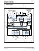
USB251xB/xBi 2.0 BLOCK DIAGRAM FIGURE 2-1: USB251XB/XBI HUB FAMILY BLOCK DIAGRAM To upstream VBUS Upstream USB data 24 MHz crystal To I2C EEPROM or SMBus master SDA SCK 3.3 V VDDA Buspower detect/ Vbus pulse Upstream PHY 1.2 V reg Serial interface PLL Serial interface engine Repeater 3.3 V ... TT #1 1.
USB251xB/xBi 3.0 PIN INFORMATION This chapter outlines the pinning configurations for each package type available, followed by a corresponding pin list organized alphabetically. The detailed pin descriptions are listed then outlined by function in Section 3.3, "Pin Descriptions (Grouped by Function)," on page 12. 3.1 Pin Configurations The following figures detail the pinouts of the various USB251xB/xBi versions.
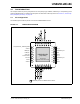
USB251xB/xBi FIGURE 3-2: USB2513B PIN DIAGRAM SUSP_IND/LOCAL_PWR/NON_REM0 28 18 PRTPWR3/BC_EN3 VDDA33 29 17 OCS_N2 USBDM_UP 30 16 PRTPWR2/BC_EN2 USBDP_UP 31 15 VDD33 XTALOUT 32 14 CRFILT XTALIN/CLKIN 33 13 OCS_N1 PLLFILT 34 12 PRTPWR1/BC_EN1 11 TEST 10 VDDA33 RBIAS 35 VDDA33 36 USB2513B/13Bi (Top View) Ground Pad (must be connected to VSS) Indicates pins on the bottom of the device. DS00001692C-page 8 2010 - 2015 Microchip Technology Inc.
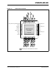
USB251xB/xBi FIGURE 3-3: USB2514B PIN DIAGRAM SUSP_IND/LOCAL_PWR/NON_REM0 28 18 PRTPWR3/BC_EN3 VDDA33 29 17 OCS_N2 USBDM_UP 30 16 PRTPWR2/BC_EN2 USBDP_UP 31 15 VDD33 XTALOUT 32 14 CRFILT XTALIN/CLKIN 33 13 OCS_N1 PLLFILT 34 12 PRTPWR1/BC_EN1 11 TEST 10 VDDA33 RBIAS 35 VDDA33 36 USB2514B/14Bi (Top View) Ground Pad (must be connected to VSS) Indicates pins on the bottom of the device. 2010 - 2015 Microchip Technology Inc.
USB251xB/xBi 3.
USB251xB/xBi TABLE 3-1: USB251XB/XBI PIN LIST (ALPHABETICAL) (CONTINUED) PRTPWR1 PRTPWR2 USB Port Power Enable 12 16 - PRTPWR3 18 - PRTPWR4 RBIAS USB Transceiver Bias 20 35 RESET_N Reset Input 26 SCL Serial Clock 24 SDA Serial Data Signal 22 SMBCLK System Management Bus Clock 24 SMBDATA System Management Bus Data Signal 22 SUSP_IND Active/Suspend Status Indicator 28 Test Pin 11 USB Bus Data 30 TEST USBDM_UP 31 USBDP_UP USBDM_DN1 Hi-Speed USB Data 1 3 USBDM_DN2 - USBDM_D
USB251xB/xBi 3.3 Pin Descriptions (Grouped by Function) An N at the end of a signal name indicates that the active (asserted) state occurs when the signal is at a low voltage level. When the N is not present, the signal is asserted when it is at a high voltage level. The terms assertion and negation are used exclusively in order to avoid confusion when working with a mixture of active low and active high signals.
USB251xB/xBi TABLE 3-2: Symbol USB251XB/XBI PIN DESCRIPTIONS (CONTINUED) Buffer Type Description SERIAL PORT INTERFACES SDA/ I/OSD12 Serial Data Signal SMBDATA/ System Management Bus Signal NON_REM1 Non-Removable Port 1 Strap Option: when enabled by package and configuration options (see Table 5-1 on page 19), this pin will be sampled (in conjunction with LOCAL_PWR/SUSP_IND/NON_REM0) at RESET_N negation to determine if ports [x:1] contain permanently attached (non-removable) devices: NON_REM[1:0] N
USB251xB/xBi TABLE 3-2: USB251XB/XBI PIN DESCRIPTIONS (CONTINUED) Symbol Buffer Type SUSP_IND/ I/O Description Active/Suspend Status LED: indicates USB state of the hub. Negated = unconfigured; or configured and in USB suspend Asserted = hub is configured and is active (i.e., not in suspend) Local Power: detects availability of local self-power source. LOCAL_PWR/ Low = self/local power source is NOT available (i.e.
USB251xB/xBi 3.3.1.1 Non-Removable If a strap pin’s buffer type is I/O, an external pull-up or pull-down must be implemented as shown in Figure 3-4. Use Strap High to set the strap option to 1 and Stap Low to set the strap option to 0. When implementing the Strap Low option, no additional components are needed (i.e., the internal pull-down provides the resistor). FIGURE 3-4: NON-REMOVABLE PIN STRAP EXAMPLE +V R k I/O Strap Pin Strap High I/O Strap Pin Strap Low R k HUB HUB GND 3.3.1.
USB251xB/xBi 3.4 Buffer Type Descriptions TABLE 3-4: BUFFER TYPE DESCRIPTIONS Buffer Type I Description Input I/O Input/output IPD Input with internal weak pull-down resistor IPU Input with internal weak pull-up resistor IS Input with Schmitt trigger O12 Output 12 mA I/O12 Input/output buffer with 12 mA sink and 12 mA source I/OSD12 ICLKx OCLKx I-R I/O-U Open drain with Schmitt trigger and 12 mA sink. Meets the I2C-Bus Specification [2] requirements.
USB251xB/xBi 4.0 BATTERY CHARGING SUPPORT The USB251xB/xBi hub provides support for battery charging devices on a per port basis in compliance with the USB Battery Charging Specification, Revision 1.1. The hub can be configured to individually enable each downstream port for battery charging support either via pin strapping as illustrated in Figure 4-1 or by setting the corresponding configuration bits via I2C EEPROM or SMBus (Section 5.1 on page 19).
USB251xB/xBi 4.2 Battery Charging Configuration The battery charging option can be configured in one of two ways: • When the hub is brought up in the default configuration with strapping options enabled, with the PRTPWR[x:1]/BC_EN[x:1] pins configured. See the following sections for details: - Section 3.3, "Pin Descriptions (Grouped by Function)," on page 12 - Section 3.3.1.2, "Internal Pull-Down (IPD)," on page 15 • When the hub is initialized for configuration over I2C EEPROM or SMBus.
USB251xB/xBi 5.0 INITIAL INTERFACE/CONFIGURATION OPTIONS The hub must be configured in order to correctly function when attached to a USB host controller. The hub can be configured either internally or externally by setting the CFG_SEL[1:0] pins (immediately after RESET_N negation) as outlined in the table below. See Chapter 11 (Hub Specification) of the USB specification for general details regarding hub operation and functionality.
USB251xB/xBi Address Register Name 06h Configuration Data Byte 1 9B 07h Configuration Data Byte 2 20 08h Configuration Data Byte 3 02 09h Non-Removable Devices 00 0Ah Port Disable (Self) 00 0Bh Port Disable (Bus) 00 0Ch Max Power (Self) 01 0Dh Max Power (Bus) 32 0Eh Hub Controller Max Current (Self) 01 0Fh Hub Controller Max Current (Bus) 32 10h Power-on Time 32 11h Language ID High 00 12h Language ID Low 00 13h Manufacturer String Length 00 14h Product String L
USB251xB/xBi 5.1.1 REGISTER 00H: VENDOR ID (LSB) Bit Number Bit Name Description 7:0 VID_LSB Least Significant Byte of the Vendor ID: a 16-bit value that uniquely identifies the Vendor of the user device (assigned by USB-Interface Forum). Set this field using either the SMBus or I2C EEPROM interface options. 5.1.
USB251xB/xBi 5.1.7 REGISTER 06H: CONFIG_BYTE_1 Bit Number Bit Name 7 SELF_BUS_PWR Description Self or Bus Power: selects between self- and bus-powered operation. The hub is either self-powered (draws less than 2 mA of upstream bus power) or bus-powered (limited to a 100 mA maximum of upstream power prior to being configured by the host controller). When configured as a bus-powered device, the hub consumes less than 100 mA of current prior to being configured.
USB251xB/xBi 5.1.8 REGISTER 07H: CONFIGURATION DATA BYTE 2 Bit Number Bit Name Description 7 DYNAMIC Dynamic Power Enable: controls the ability of the hub to automatically change from self-powered to bus-powered operation if the local power source is removed or unavailable. It can also go from bus-powered to self-powered operation if the local power source is restored. When dynamic power switching is enabled, the hub detects the availability of a local power source by monitoring LOCAL_PWR.
USB251xB/xBi 5.1.10 REGISTER 09H: NON-REMOVABLE DEVICE Bit Number Bit Name 7:0 NR_DEVICE Description Non-Removable Device: indicates which port has a non-removable device. 0 : port is removable 1 : port is non-removable Bit Bit Bit Bit Bit Bit Bit Bit 7 6 5 4 3 2 1 0 : : : : : : : : rsvd rsvd rsvd controls controls controls controls rsvd port port port port 4 3 2 1 Note: The device must provide its own descriptor data.
USB251xB/xBi 5.1.12 REGISTER 0BH: PORT DISABLE FOR BUS-POWERED OPERATION Bit Number Bit Name 7:0 PORT_DIS_BP Description Port Disable Bus-Powered: disables one or more ports.
USB251xB/xBi 5.1.15 REGISTER 0EH: HUB CONTROLLER MAX CURRENT FOR SELF-POWERED OPERATION Bit Number Bit Name Description 7:0 HC_MAX_C_SP Hub Controller Max Current Self-Powered: the value in 2 mA increments that the hub consumes from an upstream port (VBUS) when operating as a selfpowered hub. This value includes the hub silicon along with the combined power consumption (from VBUS) of all associated circuitry on the board.
USB251xB/xBi 5.1.21 REGISTER 14H: PRODUCT STRING LENGTH Bit Number Bit Name Description 7:0 PRD_STR_LEN Product String Length: with a maximum string length of 31 characters (when supported). 5.1.22 REGISTER 15H: SERIAL STRING LENGTH Bit Number Bit Name 7:0 SER_STR_LEN 5.1.23 Description Serial String Length: with a maximum string length of 31 characters (when supported).
USB251xB/xBi 5.1.26 REGISTER D0H: BATTERY CHARGING ENABLE Bit Number Bit Name 7:0 BC_EN Description Battery Charging Enable: enables the battery charging feature for the corresponding port. 0 : battery charging support is not enabled 1 : battery charging support is enabled Bit Bit Bit Bit Bit Bit Bit Bit 5.1.
USB251xB/xBi 5.1.28 REGISTER F8H: BOOST_4:0 Bit Number Bit Name 7:6 BOOST_IOUT_4 Description USB electrical signaling drive strength boost bit for downstream port 4. 00 01 10 11 5:4 BOOST_IOUT_3 BOOST_IOUT_2 BOOST_IOUT_1 5.1.
USB251xB/xBi 5.1.30 REGISTER FBH: PORTMAP 12 Bit Number Bit Name Description 7:0 PRTR12 PortMap Register for Ports 1 and 2: When a hub is enumerated by a USB host controller, the hub is only permitted to report how many ports it has; the hub is not permitted to select a numerical range or assignment. The host controller will number the downstream ports of the hub starting with the number 1, up to the number of ports that the hub reports having.
USB251xB/xBi 5.1.31 REGISTER FCH: PORTMAP 34 Bit Number Bit Name Description 7:0 PRTR34 PortMap Register for Ports 3 and 4: When a hub is enumerated by a USB host controller, the hub is only permitted to report how many ports it has; the hub is not permitted to select a numerical range or assignment. The host controller will number the downstream ports of the hub starting with the number 1, up to the number of ports that the hub reports having.
USB251xB/xBi 5.1.32 REGISTER FFH: STATUS/COMMAND Bit Number Bit Name 7:3 rsvd 2 INTF_PW_DN Description SMBus Interface Power Down: 0 : interface is active 1 : interface power down after ACK has completed 1 RESET Reset the SMBus interface and internal memory back to RESET_N assertion default settings.
USB251xB/xBi 5.2.4 IN-CIRCUIT EEPROM PROGRAMMING The EEPROM can be programmed via automatic test equipment (ATE) by pulling RESET_N low (which tri-states the hub’s EEPROM interface and allows an external source to program the EEPROM). Note: 5.3 The Hub does not have the capacity to write, or “Program,” an external EEPROM. The Hub only has the capability to read external EEPROMs.
USB251xB/xBi 5.3.2.1 Block Write/Read The block write begins with a slave address and a write condition. After the command code, the host issues a byte count which describes how many more bytes will follow in the message. If a slave had 20 bytes to send, the first byte would be the number 20 (14h), followed by the 20 bytes of data. The byte count may not be zero. A block write or read allows a transfer maximum of 32 data bytes.
USB251xB/xBi 5.3.4 STRETCHING THE SCLK SIGNAL The hub supports stretching of the SCLK by other devices on the SMBus. However, the hub does not stretch the SCLK. 5.3.5 SMBUS TIMING The SMBus slave interface complies with the SMBus Specification Revision 1.0 [3]. See Section 2.1, AC Specifications on page 3 for more information. 5.3.6 BUS RESET SEQUENCE The SMBus slave interface resets and returns to the idle state upon a START condition followed immediately by a STOP condition. 5.3.
USB251xB/xBi 5.5.1.
USB251xB/xBi 5.5.1.2 RESET_N for EEPROM Configuration FIGURE 5-2: RESET_N TIMING FOR EEPROM MODE Hardware reset asserted Read CFG_SEL[1:0] Read I2C EEPROM t1 Attach USB_RESET USB Reset Debounce USB_RESET Recovery State Interval Attach USB upstream t6 t7 t8 t9 t10 t5 t2 t3 RESET_N t4 VSS CFG_SEL[2:0] don’t care valid don’t care VSS Name t1 Description RESET_N asserted MIN t2 CFG_SEL[1:0] setup time 16.7 CFG_SEL[1:0] hold time 16.
USB251xB/xBi RESET_N for SMBus Slave Configuration 5.5.1.3 FIGURE 5-3: RESET_N TIMING FOR SMBUS MODE Hardware reset asserted Read SMBus code Hub PHY Attach USB stabilization upstream CFG_SEL[1:0] load t1 t5 t6 Attach USB_RESET USB Reset Debounce USB_RESET State Recovery Interval t7 t8 t9 t10 t2 t3 RESET_N t4 VSS CFG_SEL[2:0] don’t care valid don’t care VSS Name Description MIN TYP MAX Units t1 RESET_N Asserted 1 s t2 CFG_SEL[1:0] setup time 16.
USB251xB/xBi 6.0 DC PARAMETERS 6.1 Maximum Ratings Parameter Storage Temperature Symbol TSTOR MIN MAX Units -55 150 °C Comments Lead Temperature 3.3 V supply voltage Refer to JEDEC Specification J-STD020D [5] VDD33 VDDA33 4.6 V Voltage on any I/O pin -0.5 5.5 V Voltage on XTALIN -0.5 4.0 V Voltage on XTALOUT -0.5 2.5 V Applies to all packages Note 6-1 • Stresses above the specified parameters could cause permanent damage to the device. This is a stress rating only.
USB251xB/xBi FIGURE 6-1: SUPPLY RISE TIME MODEL Voltage tRT33 3.3 V VDD33 100% 90% VSS 10% t90% t10% Time The rise time for the 3.3 V supply can be extended to 100 ms max if RESET_N is actively driven low, typically by another IC, until 1 s after all supplies are within operating range. Note 6-2 TABLE 6-1: DC ELECTRICAL CHARACTERISTICS Parameter Symbol MIN TYP MAX Units Comments I, IS Type Input Buffer Low Input Level VILI High Input Level VIHI 0.8 2.
USB251xB/xBi TABLE 6-1: DC ELECTRICAL CHARACTERISTICS (CONTINUED) Parameter Symbol MIN TYP MAX Units 0.4 V Comments O12, I/O12 & I/OSD12 Type Buffer Low Output Level VOL High Output Level VOH IOL = 12 mA @ VDD33 = 3.3 V 2.4 V IOH = -12 mA @ VDD33 = 3.3 V Output Leakage IOL -10 +10 A Hysteresis (SD pad only) IHYSC 250 350 mV VIN = VDD33 (Note 6-1) Note 6-3 Output leakage is measured with the current pins in high impedance. Note 6-4 See USB 2.
USB251xB/xBi TABLE 6-5: SUPPLY CURRENT CONFIGURED: FULL-SPEED HOST (IFCC1) Part MIN TYP MAX Units USB2512B 45 50 mA USB2512Bi 45 55 mA USB2513B 50 55 mA USB2513Bi 50 60 mA USB2514B 50 60 mA USB2514Bi USB251xB/xBi Supply Current Configured 50 65 mA 1 port base 1 port base mA + + 8 mA 8 mA Full-Speed Host, each additional downstream port TABLE 6-6: Comments Base current of one downstream port SUPPLY CURRENT SUSPEND (ICSBY) Part MIN TYP MAX Units USB2512B 475 100
USB251xB/xBi 6.2.1 PACKAGE THERMAL SPECIFICATIONS Thermal parameters are measured or estimated for devices with the exposed pad soldered to thermal vias in a multilayer 2S2P PCB per JESD51. Thermal resistance is measured from the die to the ambient air. The values provided are based on the package body, die size, maximum power consumption, 85°C ambient temperature, and 125°C junction temperature of the die. USB2512B/12Bi USB2513B/13Bi USB2514B/14Bi (°C/W) Velocity (meters/s) JA 40.1 0 35.
USB251xB/xBi 7.0 AC SPECIFICATIONS 7.1 Oscillator/Crystal Crystal: Parallel resonant, fundamental mode, 24 MHz 350 ppm. Note: The USB251xB/xBi contains an internal 1 M resistor between the XTALIN and XTALOUT pins.
USB251xB/xBi 7.2 External Clock 50% duty cycle 10%, 24 MHz 350 ppm, jitter < 100 ps rms. The external clock is recommended to conform to the signaling level designated in the JESD76-2 Specification [5] on 1.2 V CMOS Logic. XTALOUT should be treated as a weak (<1mA) buffer output. 7.2.1 SMBUS INTERFACE The hub conforms to all voltage, power, and timing characteristics and specifications as set forth in the SMBus 1.0 Specification [3] for slave-only devices (except as noted in Section 5.
USB251xB/xBi 8.0 PACKAGE MARKING INFORMATION The following sub-sections detail the package marking information for the 36-pin SQFN and 36-pin QFN packages. To order or obtain information, e.g., on pricing or delivery, refer to the factory or the listed sales office. 8.1 36-Pin SQFN (Preferred) Example 36-Lead SQFN (6x6x0.
USB251xB/xBi 8.2 36-Pin QFN (Legacy) 36-Lead QFN (6x6x0.
2010 - 2015 Microchip Technology Inc. 9.0 Note: 9.1 PACKAGE INFORMATION For the most current package drawings, see the Microchip Packaging Specification at http://www.microchip.com/packaging. 36-Pin SQFN (Preferred) FIGURE 9-1: 36-PIN SQFN PACKAGE DRAWING http://www.microchip.
DS00001692C-page 49 FIGURE 9-2: 36-PIN QFN PACKAGE DRAWING USB251XB/XBI 36-Pin QFN (Legacy) 9.2 2010 - 2015 Microchip Technology Inc.
USB251xB/xBi APPENDIX A: ACRONYMS I2C: Inter-Integrated Circuit OCS: Over-Current Sense PCB: Printed Circuit Board PHY: Physical Layer PLL: Phase-Locked Loop QFN: Quad Flat No Leads RoHS: Restriction of Hazardous Substances Directive SCL: Serial Clock SIE: Serial Interface Engine SMBus: System Management Bus TT: Transaction Translator DS00001692C-page 50 2010 - 2015 Microchip Technology Inc.
USB251xB/xBi APPENDIX B: 1. 2. 3. 4. 5. REFERENCES Universal Serial Bus Specification, Version 2.0, April 27, 2000 (12/7/2000 and 5/28/2002 Errata) USB Implementers Forum, Inc. http://www.usb.org I2C-Bus Specification Version 1.1 NXP (formerly a division of Philips). http://www.nxp.com System Management Bus Specification, version 1.0 SMBus. http://smbus.org/specs/ MicroChip 24AA02/24LC02B (Revision C) Microchip Technology Inc. http://www.microchip.
USB251xB/xBi APPENDIX C: TABLE C-1: DATA SHEET REVISION HISTORY REVISION HISTORY Revision Level & Date DS00001692C (10-20-15) Section/Figure/Entry Product Identification System Correction PIS ordering code information for preferred package corrected to align with current Microchip standard practices. Section 8.0, "Package Marking Top marking diagrams corrected to be consistent Information" with internal specifications and current physical part markings.
USB251xB/xBi TABLE C-1: REVISION HISTORY (CONTINUED) Revision Level & Date Section/Figure/Entry Correction Section 1.1, "Configurable Features," on page 4 Updated bulleted lists. USB signal drive strength, USB differential pair pin location and downstream port power control / over-current detection items moved from first (strap-configurable) bulleted list to the second (EEPROM-configurable) bulleted list. Added enabling of battery charging to the first bulleted list. Section 3.
USB251xB/xBi THE MICROCHIP WEB SITE Microchip provides online support via our WWW site at www.microchip.com. This web site is used as a means to make files and information easily available to customers.
USB251xB/xBi PRODUCT IDENTIFICATION SYSTEM The USB251xB/xBi is available in a 36-pin SQFN (preferred) and 36-pin QFN (legacy) package. For new designs, the 36-pin SQFN is recommended. The ordering code information varies dependent on the package selected. The following sub-sections detail the product identification system for the 36-pin SQFN (preferred) and 32-pin QFN (legacy). To order or obtain information, e.g., on pricing or delivery, refer to the factory or the listed sales office.
Note the following details of the code protection feature on Microchip devices: • Microchip products meet the specification contained in their particular Microchip Data Sheet. • Microchip believes that its family of products is one of the most secure families of its kind on the market today, when used in the intended manner and under normal conditions. • There are dishonest and possibly illegal methods used to breach the code protection feature.
Worldwide Sales and Service AMERICAS ASIA/PACIFIC ASIA/PACIFIC EUROPE Corporate Office 2355 West Chandler Blvd. Chandler, AZ 85224-6199 Tel: 480-792-7200 Fax: 480-792-7277 Technical Support: http://www.microchip.com/ support Web Address: www.microchip.