
Datasheet


2010 - 2015 Microchip Technology Inc. DS00001692C-page 7
USB251xB/xBi
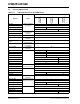
3.0 PIN INFORMATION
This chapter outlines the pinning configurations for each package type available, followed by a corresponding pin list
organized alphabetically. The detailed pin descriptions are listed then outlined by function in Section 3.3, "Pin Descrip-
tions (Grouped by Function)," on page 12.
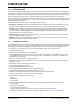
3.1 Pin Configurations
The following figures detail the pinouts of the various USB251xB/xBi versions.
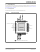
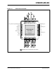
FIGURE 3-1: USB2512B PIN DIAGRAM
Ground Pad
(must be connected to VSS)
USB2512B/12Bi
(Top View)
18
NC
17
16
15
14
VDD33
13
CRFILT
12
11
TEST
10
VDDA33
OCS_N2
PRTPWR2/BC_EN2
OCS_N1
PRTPWR1/BC_EN1
28
VDDA33
29
USBDP_UP
31
XTALOUT
32
33
RBIAS
36
VDDA33
35
PLLFILT
34
USBDM_UP
30
XTALIN/CLKIN
SUSP_IND/LOCAL_PWR/NON_REM0
Indicates pins on the bottom of the device.