
User's Manual


MICROELECTRONICS TECHNOLOGY INC 2 September 15, 2017
Table of Contents
1 Introduction ................................................................................................................................................. 3
2 Regulatory Statement ................................................................................................................................. 4
3 System Block Diagram ................................................................................................................................. 6
4 Specifications ............................................................................................................................................... 7
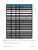
5 Pin Configurations and Descriptions ........................................................................................................... 8
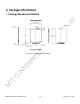
6 Package Information ................................................................................................................................. 10
Package Mechanical Outline ..................................................................................................... 10
7 Interfacing to the PCIe M.2 Module .......................................................................................................... 11
8 Operating the PCIe M.2 Module ............................................................................................................... 12
9 Revision History ......................................................................................................................................... 13
Figures
Figure 1: System Block Diagram ......................................................................................................................... 6
Figure 2: Pin Configurations ............................................................................................................................... 8
Figure 3: Package Mechanical Outline.............................................................................................................. 10
Tables
Table 1: Band configurations .............................................................................................................................. 3
Table 2: Specifications ........................................................................................................................................ 7
Table 3: Pin Configurations ................................................................................................................................. 9
Table 4: Revision history ................................................................................................................................... 13