
Operating Manual


HP900 Operating Manual 5
Once the equipment is deployed, you can verify the signal strength by
entering into Command Mode and reading Register S123. This register
provides the average signal strength in dBm. The minimum strength for
communication is roughly -108dBm. For consistent reliable
communication, you should try to deploy the equipment such that signal
strength exceeds -95dBm.
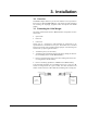
3.2 Antennas and Cabling
This section describes the recommended procedure for PCB design for the
Antenna Connector and installing cabling and antennas for use with the
HP900 module.
3.2.1 PCB Requirements for Antenna Interface
The HP900 provides an RF interface for connecting an external antenna
through a PCB pad (#45 RF_Antenna) for RF signal transmission and
reception. A PCB must be designed that incorporates a 50 Ω trace to a RP-
SMA connector for the HP900 to interface to an external antenna. A high
quality 50 Ω RF connector, such as a RP-SMA connector, provides proper
PCB-to RF-cable transition.
Proper transition between RF_Antenna pad and the application board PCB
must be provided by following the design guidelines for the layout of the
application PCB close to the RF_Antenna pad:
• On a multilayer board, the layer stack below the RF connection
should be free of digital lines
• Increase GND clearance around the RF_Antenna pad, on the top
layer of the PCB, to at least 250 μm up to adjacent pads metal
definition and up to 400 μm on the area below the module, to
reduce parasitic capacitance to ground.
• Add GND clearance on the buried metal layer below the
RF_Antenna pad if the top-layer to buried layer dielectric
thickness is below is below 200 μm, to reduce parasitic capacitance
to ground.
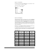
3.2.2 PCB Requirements for RF Transmission line design
Any RF transmission line, such as the ones from the RF_Antenna pad up
to the related antenna connector or up to the related internal antenna pad,
must be designed so that the characteristic impedance is as close as possible
to 50 Ω.
The following figures provide two examples of proper 50 Ω coplanar
waveguide designs. The first example is of a RF transmission line
implemented in a 4-layer PCB, and the second is an example of a RF
transmission line implemented in a 2-layer PCB.