
Information


Electrical characteristics STM32F20xxx
112/178 DocID15818 Rev 11
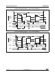
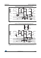
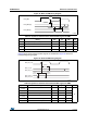
Figure 41. SPI timing diagram - slave mode and CPHA = 0
Figure 42. SPI timing diagram - slave mode and CPHA = 1
ai14134c
SCK Input
CPHA= 0
MOSI
INPUT
MISO
OUT P UT
CPHA= 0
MS B O U T
MSB IN
BI T6 OU T
LSB IN
LSB OUT
CPOL=0
CPOL=1
BIT1 IN
NSS input
t
SU(NSS)
t
c(SCK)
t
h(NSS)
t
a(SO)
t
w(SCKH)
t
w(SCKL)
t
v(SO)
t
h(SO)
t
r(SCK)
t
f(SCK)
t
dis(SO)
t
su(SI)
t
h(SI)
ai14135
SCK Input
CPHA=1
MOSI
INPUT
MISO
OUT P UT
CPHA=1
MS B O U T
MSB IN
BI T6 OU T
LSB IN
LSB OUT
CPOL=0
CPOL=1
BIT1 IN
t
SU(NSS)
t
c(SCK)
t
h(NSS)
t
a(SO)
t
w(SCKH)
t
w(SCKL)
t
v(SO)
t
h(SO)
t
r(SCK)
t
f(SCK)
t
dis(SO)
t
su(SI)
t
h(SI)
NSS input