
Information

DocID15818 Rev 11 149/178
STM32F20xxx Electrical characteristics
177
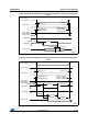
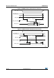
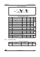
Figure 75. SD default mode
6.3.28 RTC characteristics
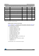
Table 85. SD / MMC characteristics
Symbol Parameter Conditions Min Max Unit
f
PP
Clock frequency in data transfer
mode
C
L
≤ 30 pF 0 48 MHz
- SDIO_CK/f
PCLK2
frequency ratio - - 8/3 -
t
W(CKL)
Clock low time, f
PP
= 16 MHz C
L
≤ 30 pF 32
ns
t
W(CKH)
Clock high time, f
PP
= 16 MHz C
L
≤ 30 pF 31
t
r
Clock rise time C
L
≤ 30 pF 3.5
t
f
Clock fall time C
L
≤ 30 pF 5
CMD, D inputs (referenced to CK)
t
ISU
Input setup time C
L
≤ 30 pF 2
ns
t
IH
Input hold time C
L
≤ 30 pF 0
CMD, D outputs (referenced to CK) in MMC and SD HS mode
t
OV
Output valid time C
L
≤ 30 pF 6
ns
t
OH
Output hold time C
L
≤ 30 pF 0.3
CMD, D outputs (referenced to CK) in SD default mode
(1)
1. Refer to SDIO_CLKCR, the SDI clock control register to control the CK output.
t
OVD
Output valid default time C
L
≤ 30 pF 7
ns
t
OHD
Output hold default time C
L
≤ 30 pF 0.5
ai14888
CK
D, CMD
(output)
t
OVD
t
OHD
Table 86. RTC characteristics
Symbol Parameter Conditions Min Max
-f
PCLK1
/RTCCLK
frequency ratio
Any read/write operation
from/to an RTC register
4-