
User's Manual


2 - 10
2. DEVICE RANGE THAT CAN BE SET
2.3 MELSEC-QnA/Q/QS, MELDAS C6 *
2.3 MELSEC-QnA/Q/QS, MELDAS C6 *
The device ranges that can be set when selecting
[MELSEC-QnA/Q/QS, MELDAS C6*]
*13
as the controller
type are as follows.
*1 Do not set a file register by GT Designer3 when executing
multiple programs with the file of the file register set at [Use
the same file name as the program] by the PLC parameter of
GX Developer.(Except MELSEC-QnA)
Otherwise, read/write at GOT will be erroneous.
*2 Available for file register of block No. switched with the RSET
instruction.
*3 Available for file register of block No. of file name switched
with the QDRSET instruction.
*4 GOT treats them in units of 32k (32768 points).
*5 Only the intelligent function module on the station connected
to GOT can be specified.
Set within the address range of the buffer memory existing in
the target intelligent function module.
*6 The device No. must be set in multiples of 16.
*7 When monitoring MELDAS C6/64, if a word device outside
the range is set, the value becomes indefinite.
When a bit device outside the range is set, the object may
not be displayed or the set function may fail to operate.
Check the set device using the device list of GT Designer3.
*8 Devices used by the MELDAS C6/64 system cannot be
used.
*9 Do not use local devices set in the MELSEC-Q system.
Otherwise, normal monitoring is not performed.
*10 This is not supported by GT10.
*11 This cannot be monitored when in GOT multi-drop
connection.
*12 Only reading is possible from QS001CPU.
*13 For GT14, GT11 and GT10, the controller type is as follows.
• GT14, GT11: MELSEC-QnA/Q, MELDAS C6 *
• GT10: MELSEC-QnA/Q
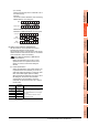
Device name
*7 *8 *12
Setting range
Device No.
representation
Bit device
Input (X) X0 to X3FFF
Hexadecimal
Output (Y) Y0 to Y3FFF
Internal relay (M)
*9
M0 to M32767
Decimal
Latch relay (L) L0 to L32767
Annunciator (F) F0 to F32767
Link relay (B) B0 to B7FFF
Hexadecimal
Timer
*9
Contact (TT) TT0 to TT32767
Decimal
Coil (TC) TC0 to TC32767
Counter
*9
Contact (CT) CT0 to CT32767
Coil (CC) CC0 to CC32767
Special relay (SM) SM0 to SM2047
Retentive
timer
*9
Contact (SS) SS0 to SS32767
Coil (SC) SC0 to SC32767
Step relay (S) S0 to S32767
Link special relay (SB) SB0 to SB7FFF
Hexadecimal
Word device bit
Specified bit of the
following word devices
(Except Timer, Counter,
Retentive timer, Index
register and Buffer
memory)
―
Word device
Data register (D)
*9
D0 to D32767
Decimal
Special data register (SD) SD0 to SD2047
Link register (W) W0 to W7FFF
Hexadecimal
Timer (current value) (TN)
*9
TN0 to TN32767
Decimal
Counter (current value)
(CN)
*9
CN0 to CN32767
Retentive timer
(current value) (SN)
*9
SN0 to SN32767
Link special register (SW) SW0 to SW7FFF
Hexadecimal
File register (R)
*1*2
R0 to R32767
Decimal
Extension
file register
(ER)
*1*10*11
Block 0 to 255
Device R0 to R32767
Extension file register
(ZR)
*1*3*4*10*11
ZR0 to
ZR1042431
Index register (Z) Z0 to Z15
Buffer memory
(Intelligent function module)
(BM)
*5*10*11
BM0 to BM32767
Buffer memory
(Intelligent function module)
(G)
*4*5*10*11
G0 to G65535
Ww
*10*11
Ww0 to Ww1FFF
Hexadecimal
Wr
*10*11
Wr0 to Wr1FFF
Bit device word
*6*10
Converting the above bit
devices into words
(Except Timer, Counter
and Retentive timer)
―