
Instruction manual

25
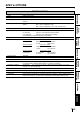
FEATURES &
FUNCTIONS
PRECAUTIONS
SPECIAL
FEATURES &
UNPACKING
CONNECTIONS
BEFORE
OPERATION
TROUBLE-
SHOOTING
CLEANING
OTHERS
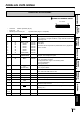
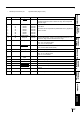
PARALLEL DATA SIGNAL
• Connector JD36SL equivalent (36-pin)
• Input level TTL
• Parallel input connector port Signal allocation (Signal : Compatible)
Pin No.
1
2
3
4
5
6
7
8
9
10
11
12
13
14
16•17
18
19 - 30
31
32
15•
33 - 35
36
Return pin No.
19
20
21
22
23
24
25
26
27
28
29
16
Signal
STROBE
DATA1 (LSB)
DATA2
DATA3
DATA4
DATA5
DATA6
DATA7
DATA8 (MSB)
ACK
(ACKNOWLEDGE)
BUSY
P•E
(PAPER END)
SELECT
AutoFd
GND
High
GND
Init
Fault
NC
SelectIn
From/To
PC/VCP
PC/VCP
PC/VCP
PC/VCP
PC/VCP
PC/VCP
PC/VCP
PC/VCP
PC/VCP
PC/VCP
PC/VCP
PC/VCP
PC/VCP
PC/VCP
PC/VCP
PC/VCP
PC/VCP
PC/VCP
PC/VCP
Function
Strobe pulse for data reading. Incoming pulse width should be
0.5µs minimum. At regular conditions, “High” data will be read after
becoming “Low”.
High: data 1
Low: data 0
Information will be expressed for parallel data of every signal from
bit No.1 to No.8.
The signal is yielded after data input has ended by a data
reception acknowledgement pulse.
High: VCP data is not accepted.
Low : VCP data is accepted.
The signal becomes “High” in the following cases:
• On OFF LINE status
• During data entry
High: No paper
Low : Paper available
High : When ON LINE switch is ON
Low : When ON LINE switch is OFF
High
Earth
PeripheralLogicHigh
Earth
Clears sending data to this unit. (Low) Incoming pulse width
should be 100µs minimum.
Low : Abnormal condition occurs in VCP. (e.g. error due to paper
jamming, etc.)
Unused
Low
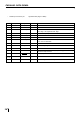
PARALLEL TERMINAL SIGNAL
Pin number
19
36
118
PARALLEL DATA SIGNAL