
Service manual


I²C-bus autosync deflection controller for PC monitors TDA4857
66
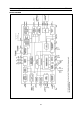
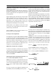
An internal discharge circuit allows a well defined discharge
of capacitors at BSENS. BDRV is active at a LOW-level
output voltage (see Fig. 22), thus it requires an external
inverting driver stage.
The B+ function block can be used for B+ deflection modu-
lators in many different ways. Two popular application com-
binations are as follows:
• Boost converter in feedback mode (see Fig. 22)
In this application the OTA is used as an error amplifier
with a limited output voltage range. The flip-flop is set on
the rising edge of the signal at HDRV. A reset will be
generated when the voltage at BSENS, taken from the
current sense resistor, exceeds the voltage at BOP.
If no reset is generated within a line period, the rising
edge of the next HDRV pulse forces the flip-flop to reset.
The flip-flop is set immediately after the voltage at BSENS
has dropped below the threshold voltage V
RESTART(BSENS).
• Buck converter in feed forward mode
This application uses an external RC combination at
BSENS to provide a pulse width which is independent
from the horizontal frequency. The capacitor is charged
via an external resistor and discharged by the internal
discharge circuit. For normal operation the discharge
circuit is activated when the flip-flop is reset by the inter-
nal voltage comparator. The capacitor will now be dis-
charged with a constant current until the internally con-
trolled stop level V
STOP(BSENS) is reached. This level will
be maintained until the rising edge of the next HDRV
pulse sets the flip-flop again and disables the discharge
circuit.
If no reset is generated within a line period, the rising
edge of the next HDRV pulse automatically starts the
discharge sequence and resets the flip-flop. When the
voltage at BSENS reaches the threshold voltage
VRESTART(BSENS), the discharge circuit will be disabled au-
tomatically and the flip-flop will be set immediately. This
behaviour allows a definition of the maximum duty cycle
of the B+ control drive pulse by the relationship of charge
current to discharge current.
Supply voltage stabilizer, references, start-up
procedures and protection functions
The TDA4857 provides an internal supply voltage stabi-
lizer for excellent stabilization of all internal references. An
internal gap reference, especially designed for low-noise,
is the reference for the internal horizontal and vertical sup-
ply voltages. All internal reference currents and drive cur-
rent for the vertical output stage are derived from this volt-
age via external resistors.
If eithr the supply voltage is below 8.3V or no data from the
I²C-bus has been received after power-up, the internal soft
start and protection functions fo not allow any of those out-
puts [HDRV, BDRV, VOUT1, VOUT2 and HUNLOCK] to
be active.
For supply voltages below 8.3V the internal I²C-bus will not
generated an acknowledge and the IC is in standby mode.
This is because the internal protection circuit has gener-
ated a reset signal for the soft start register SOFTST. Above
8.3V data is accepted and all registers can be loaded. If the
register SOFTST has received a set from the I²C-bus, the
internal soft start procedure is released, which activates all
above mentioned outputs.
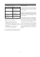
If during normal operation the supply voltage has dropped
below 8.1 V, the protection mode is activated and
HUNLOCK (pin 17) changes to the protection status and is
floating. This can be detected by the microcontroller.
This protection mode has been implemented in order to
protect the deflection stages and the picture tube during
start-up, shut-down and fault conditions. This protection
mode can be activated as shown is Table 3.