
User`s manual


8 - 3 8 - 3
MELSEC-Q
8 TROUBLESHOOTING
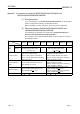
8.2.3 When an analog output value is not output
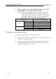
Check item Action to be taken
Is 24VDC external power supply being supplied?
Verify that 24VDC voltage is being supplied to the external power
supply terminals
(Q62DAN, Q64DAN, Q62DA, Q64DA: terminal numbers 16, 17
Q68DAVN, Q68DAIN, Q68DAV, Q68DAI: terminal numbers 17, 18).
Is there any fault with the analog signal lines
such as broken or disconnected line?
Check for any abnormality on the signal lines by doing a visual check
and performing a continuity check.
Is the CPU module in the STOP status? Set the CPU module to the RUN status.
Are the offset/gain settings correct?
Verify that the offset/gain settings are correct (see sections 4.6, 5.6.2
and 5.6.3).
If the user range setting is being used, switch to a different default
input range and check if D/A conversion is correctly performed. If it is
correctly performed, redo the offset/gain settings.
Is the output setting range correct?
Verify buffer memory address 20 and 21 (Un\G20 and Un\G21) in GX
Developer monitor. If the output range setting is incorrect, redo GX
Developer intelligent function module switch settings (see Section
4.5).
Is the resolution mode setting correct?
Check the ON/OFF status of the high resolution mode status flag (X8)
in GX Developer system monitor.
If the resolution mode setting is incorrect, redo the GX Developer
intelligent function module switch setting. (See Section 4.5.)
Is the D/A conversion enable/disable setting for
the channel to be output set to Disable?
Check the D/A conversion enable/disable setting using buffer memory
0 (Un\G0) in GX Developer monitor and set it to Enable using the
sequence program or utility package (see Section 3.4).
Is the D/A output enable/disable setting for the
channel to be output set to Disable?
Verify ON/OFF for the output enable/disable flags (Y1 to Y8) in GX
Developer monitor.
If the output enable/disable flags are OFF, review the initial setting for
the sequence program or utility package (see Section 3.3).
Is the digital value being written to the channel to
be output?
Verify buffer memory addresses 1 to 8 (Un\G1 to Un\G8) in GX
Developer monitor (see Section 3.4).
Has the operating condition setting request (Y9)
been executed?
Set the operating condition setting request (Y9) from ON to OFF from
GX Developer and check to see if the analog output is normal.
If normal analog output is obtained, review the initial setting for the
sequence program or utility package (see Section 3.3).
POINT
If the analog output value is not output after the proper corrective action is taken in
accordance with the above check item, the possible cause is a module failure.
Consult the nearest sales representative or branch.