FSC-BT645 Datasheet S BLE 4.2 Single Mode Bluetooth Module Datasheet Version 1.1 Shenzhen Feasycom Technology Co.,Ltd -1- www.feasycom.
FSC-BT645 Datasheet Copyright © 2013-2019 Feasycom Technology. All Rights Reserved. Feasycom Technology reserves the right to make corrections, modifications, and other changes to its products, documentation and services at anytime. Customers should obtain the newest relevant information before placing orders. To minimize customer product risks, customers should provide adequate design and operating safeguards.
FSC-BT645 Datasheet Contents 1. INTRODUCTION ............................................................................................................................................................... 4 2. GENERAL SPECIFICATION ................................................................................................................................................. 5 3. HARDWARE SPECIFICATION .........................................................................................................
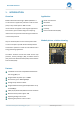
FSC-BT645 Datasheet 1. INTRODUCTION Overview Application BT645 is Bluetooth Low Energy 4.2(BLE4.2) Module. It Health Thermometer can be used as an application processor as well as a data Heart Rate pump in fully hosted systems. MCU is 32-bit Blood Pressure microcontroller. It supports a wide range of applications Proximity from low-end, price sensitive designs to computing- Human Interface Device (HID) intensive ones and provides advanced high-end features in economical products.
FSC-BT645 Datasheet 2. General Specification Table 1: General Specifications Categories Wireless Specification Features Implementation Bluetooth Version Bluetooth low energy 4.2 Frequency 2.402 - 2.480 GHz Transmit Power 1.
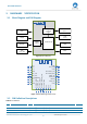
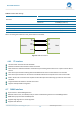
FSC-BT645 Datasheet 3. HARDWARE SPECIFICATION 3.1 Block Diagram and PIN Diagram Internal(Default) or external antenna UART Antenna (optional) J-Link I2C/SPI (optional) 16MHZ Crystal PIOs/AIOs Bluetooth Chip Wake VDD 2.2V ~ 3.6V Reset Figure 2: Block Diagram GND 28 EXT_ANT GND 27 26 25 P1.5/UART_RTS 24 6 ICE_DAT P0.2 10 GND P0.7 UART_TX 23 UART_RX 22 RESET 21 VDD_3V3 20 GND 19 P2.6 8 9 P3.6/SPI1_SS P5.2/WAKEUP P1.0/SPI1_MOSI 7 P2.5 P1.4/UART_CTS ICE_CLK P0.
FSC-BT645 Datasheet 4 GND Vss Power Ground 5 ICE_CLK I/O Debugging through the CLK line(Default) Note 1 6 ICE_DAT I/O Debugging through the DATA line(Default) Note 1 7 P5.2/WAKEUP I/O Programmable input/output line Alternative Function: Wake up = Hight level(Default) 8 P0.2 I/O Programmable input/output line Alternative Function: LED(Default) Note 1,4 9 P0.7 I/O Programmable input/output line Alternative Function: BT Status(Default) Note 1,2 10 GND Vss Power Ground 11 P1.
FSC-BT645 Datasheet Note 4 Note 5 Note 6 LED(Default)-- Power On: Light Slow Shinning ; Connected: Steady Lighting. By default, this PIN is an empty feet. This PIN can connect to an external antenna to improve the Bluetooth signal coverage. If you need to use an external antenna, by modifying the module on the 0R resistance to block out the on-board antenna; Or contact Feasycom for modification. This I / O port is shared with the internal SPI Flash chip.
FSC-BT645 Datasheet 4.4 General Purpose Digital IO There are 11 general purpose digital IOs defined in the module. All these GPIOs can be configured by software to realize various functions, such as button controls, LED drives or interrupt signals to host controller, etc. Do not connect them if not use. The I/O type of each I/O pins can be configured by software individually as Input or Push-pull output mode.
FSC-BT645 Datasheet Table 3: Possible UART Settings Parameter Possible Values Baudrate Minimum 1200 baud (≤2%Error) Standard 115200bps(≤1%Error) Maximum 921600bps(≤1%Error) Flow control RTS/CTS, or None Parity None, Odd or Even Number of stop bits 1 /1.5/2 Bits per channel 5/6/7/8 When connecting the module to a host, please make sure to follow . Module TX RX RX TX RTS CTS CTS RTS GND GND Host Figure 4: UART Connection 4.6.
FSC-BT645 Datasheet 5. ELECTRICAL CHARACTERISTICS 5.1 Absolute Maximum Ratings Absolute maximum ratings for supply voltage and voltages on digital and analogue pins of the module are listed below. Exceeding these values causes permanent damage. The average PIO pin output current is defined as the average current value flowing through any one of the corresponding pins for a 100mS period.
FSC-BT645 Datasheet DR Data rate △f1M Frequency deviation FCH1M Channel spacing - 1 - Mbps 225 250 275 KHz - 2 - MHz -18 - 13 dBm Transmitter PRF Output power PBW 20dB Bandwidth for Modulated Carrier at 1Mbps - 1.5 - MHz RXmax Maximum received signal at <0.1% BER - -10 - dBm RXSENS Sensitivity (0.
FSC-BT645 Datasheet (2) JEDEC document JEP155 states that 500-V HBM allows safe manufacturing with a standard ESD control process. (3) JEDEC document JEP157 states that 250-V CDM allows safe manufacturing with a standard ESD control process. 7. RECOMMENDED TEMPERATURE REFLOW PROFILE Prior to any reflow, it is important to ensure the modules were packaged to prevent moisture absorption.
FSC-BT645 Datasheet ℃ 250 217 210 A 25 0 B 1 2 C 3 D 4 E 5 6 min Figure 5: Typical Lead-free Re-flow Pre-heat zone (A) — This zone raises the temperature at a controlled rate, typically 0.5 – 2 C/s. The purpose of this zone is to preheat the PCB board and components to 120 ~ 150 C. This stage is required to distribute the heat uniformly to the PCB board and completely remove solvent to reduce the heat shock to components.
FSC-BT645 Datasheet Figure 6: BT645 footprint 9. HARDWARE INTEGRATION SUGGESTIONS 9.1 Soldering Recommendations BT645 is compatible with industrial standard reflow profile for Pb-free solders. The reflow profile used is dependent on the thermal mass of the entire populated PCB, heat transfer efficiency of the oven and particular type of solder paste used. Consult the datasheet of particular solder paste for profile configurations.
FSC-BT645 Datasheet 20 25 5 13 Max.0.5 18 43.5 Max.0.5 no bare copper(exept solder pads for module) 10 no copper and components on any layer no components on any layer 20 10 Applic. PCB do not place any conductive parts in this area Provide solid ground plane(s) as large as possible around area Figure 7: BT645 Restricted Area Following recommendations helps to avoid EMC problems arising in the design.
FSC-BT645 Datasheet Antenna Antenna Non enmitting circuits RF & heat enmitting circuits Non enmitting circuits Digital Part RF & heat enmitting circuits RF_IN RF_IN Digital Part Digital & Analog Circuits Digital & Analog Circuits PCB PCB Figure 8: Placement the Module on a System Board 9.3.
FSC-BT645 Datasheet Antenna Wrong Antenna Antenna PCB PCB PCB Better Best Figure 10: Recommended Trace Connects Antenna and the Module Routing of the RF-connection underneath the module should be avoided. The distance of the micro strip line to the ground plane on the bottom side of the receiver is very small and has huge tolerances. Therefore, the impedance of this part of the trace cannot be controlled. Use as many vias as possible to connect the ground planes. 10.
FSC-BT645 Datasheet Figure 11: Tray vacuum 10.2 Packing box(Optional) * If require any other packing, must be confirmed with customer * Package: 1000PCS Per Carton (Min Carton Package) Figure 12: Packing Box Shenzhen Feasycom Technology Co.,Ltd -19- www.feasycom.
FSC-BT645 Datasheet Please take attention that changes or modification not expressly approved by the party responsible for compliance could void the user’s authority to operate the equipment. This device complies with Part 15 of the FCC Rules. Operation is subject to the following two conditions: (1) This device may not cause harmful interference, and (2) This device must accept any interference received, including interference that may cause undesired operation.