
Data Sheet

FSC-BT645 Datasheet
Shenzhen Feasycom Technology Co.,Ltd www.feasycom.com
-11-
5. ELECTRICAL CHARACTERISTICS
5.1 Absolute Maximum Ratings
Absolute maximum ratings for supply voltage and voltages on digital and analogue pins of the module are listed below.
Exceeding these values causes permanent damage.
The average PIO pin output current is defined as the average current value flowing through any one of the corresponding
pins for a 100mS period. The total average PIO pin output current is defined as the average current value flowing through
all of the corresponding pins for a 100mS period. The maximum output current is defined as the value of the peak current
flowing through any one of the corresponding pins.
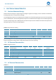
Table 4: Absolute Maximum Rating
Symbol
Description
Min
Trp
Max
Unit
VDD
BT Input voltage
-0.3
-
3.6
V
VI
Input voltage
-0.3
-
VDD
V
VO
Output voltage
VSS
-
VDD
V
TOP
Operating Temperature
-40
-
85
°C
TSTG
Storage Temperature
-40
-
125
°C
Note: Exceeding one or more of the limiting values may cause permanent damage to BT645.
Caution: Electrostatic sensitive device, comply with protection rules when operating.
5.2 DC Electrical Characteristics
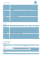
Table 5: Voltage and current
Symbol
Parameter
Min
Type
Max
Unit
Test Conditions
V
DD
-V
SS
-
DC Power Supply
2.2
3
3.6
V
TA=25°C
T
A
-
Operating Temperature
-40
25
+85
°C
-
I1
Standby Current in Sleep mode
-
8
-
uA
Wakeup PAD or RESET
VOH
Output high level voltage
VDD-0.3
-
VDD
V
-
VOL
Output low level voltage
VSS
-
VSS+0.3
V
-
VIH
Input high level voltage
2.0
3
3.6
V
-
VIL
Input low level voltage
VSS
-
VSS+0.3
V
-
5.3 AC Electrical Characteristics
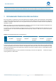
Table 6: RF
Symbol
Parameter
Min
Type
Max
Unit
General frequency
Fop
Operating frequency
2402
-
2480
MHz
PLLres
PLL Programming resolution
-
1
-
MHz
Fxtal
Crystal frequency
-
16
-
MHz