
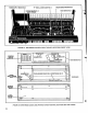
Service manual


shunts
varying
proportions
of
oscillators
A
and
B
to
ground.
The
values
of
resistors
R522
thru
R525
relative
to
the
value
of
the
A/B
MIX
control
are
set
so
that
the
signal
power
sum
at
pins
Z
and
ZZ
tends
to
remain
constant
as
the
A/B
MIX
control
is
rotated.
The
output
at
pin
Z
is
the
oscillator
A
signal
applied
to
the
normal
input
portion
of
the
band
pass
filter
via
R122
and
R124.
The
output
at
pin
ZZ
is
the
oscillator
B
signal
applied
further
down
the
chain
of
the
band
pass
filter
to
produce
a
different
sound
character.
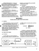
2.5
BAND
PASS
FILTER
The
band
pass
filter
consists
of
IC15,
IC16
and
IC17
with
associated
components.
IC16
and
IC17
are
identical
integrators
effectively
connected
in
series
and
their
gains
determine
the
center
frequency
of
the
band
pass
filter
while
the
gain
of
IC15
determines
the
bandwidth
(Q).
These
gains
are
set
by
bias
currents
applied
from
transistor
pairs
Q39/Q40
and
Q37/Q38,
respectively.
These
transistor
pairs
may
be
compared
directly
to
the
transistor
pair
in
ICll
which
determines
the
frequency
of
oscillation.
The
main
difference
is
that
relatively
constant
currents
are
fed
to
these
transistor
pairs
through
R133
and
R129.
A
precise,
wide
range
relationship
between
output
current
and
base-to-base
voltage
is
not
required
of
these
transistor
pairs.
Only
reasonable
repeatability
and
the
rough
approximation
of
exponential
characteristics
are
required.
2.5.1
BAND
PASS
FILTER
CONTROL
INPUTS
The
bandwidth
is
determined
by
the
voltage
difference
between
the
bases
of
Q37
and
Q38.
The
voltage
at
the
base of
Q37
is
the
result
of
the
band
width
control current
flowing
through
R128.
An
increase
of
18.5
mv
doubles
the
bandwidth.
The
one
source of
bandwidth
control current
is
column
8
of
the
resistor
matrix.
The
center
frequency
is
deter
mined
by
the
voltage
difference
between
the
bases
of
Q39
and
Q40.
The
voltage
at
the
base
of
Q40
is
the
result
of the center
frequency
control
currents
flowing
through
R134.
An
increase
of
18.5
mv
doubles
the
center
frequency.
The
currents
come
from
column
7
of
the
resistor
matrix,
the
BRIGHTNESS
potentiometer
voltage
applied
to
R193,
the
FILTER
CONTROL
INPUT
jack
voltage
applied
to
R184,the
modulation
voltage
applied
to
R181,
the
filter
contour
voltage
applied
to
R116
and
the
keyboard
pitch
voltage
applied
through
R179
and
R180.
The
current
from
column
4
of
the
resistor
matrix
deter
mines
whether
or
not
Q25
conducts.
When
Q25
conducts,
it
becomes
saturated
and
shorts
out
the
keyboard
voltage
controlling
the
center
frequency.
R130
and
R132
are
offset
adjustments
for
setting
correct
values
of
bandwidth and
center
frequency,
respectively
and
compensate
for
transistor
offset
voltages,
resistor
variations
and
gain
variations
of
IC15,
IC16
and
IC17.
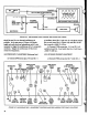
2.6
LOW
PASS
FILTER
The
output
of
the
band
pass
filter
is
taken
from
the
source
of
Q41
and
applied
across
the
bases
of
the
bottom
transistor
pair
of
IC19.
This
transistor
pair
and
the
two
immediately
following
it
constitute
a
low
pass
filter
whose
cutoff
frequency
is
proportional
to
the
standing
current.
This
current
is
determined
by
the
voltage
difference
between
pin
13
(ground)
of
IC19
and
the
base
of
Q33.
The
voltage
at
the
base
of
Q33
is
the
result
of
cutoff
frequency
currents
flowing
through
R151.
These
currents
come
from
column
9
of
the
resistor
matrix,
the
BRIGHTNESS
potentiom
eter
voltage
applied
to
R186,
FILTER
CONTROL
INPUT
jack
voltage
applied
to
R185,
modulation
voltage
applied
to
R187
and
filter
contour
voltage
applied
through
R117.
The
setting
of
R139
deter
mines
the
calibration
current
through
R140.
An
increase
of
approximately
18.5
mv
at
the
base
of
Q33
results
in
a
one
octave
increase
in
the cutoff
frequency
of
the
low
pass
filter.
2.7
VOLTAGE
CONTROLLED
AMPLIFIER
The
transistor
pair
with
common
emitters
on
pin
3
of
IC20
controls
the
amplitude
of
the
audio
wave
form by
variable
transconductance.
The
current
which
determines
this
transconductance
is
determined
by
the
voltage
at
pin
12
of
IC20
and
the
resistance
between
pin
13
and
ground.
The
voltage
applied
to
pin
12
is
the
amplitude
contour
voltage
and
the
resistance
from
pin
B19
to
ground
is
the
100K
VOLUME
control
potentiometer.
IC22
is
a
differential
amplifier,
the
output
of
which
is
the
final
audio
waveform.
20