
Service manual


June, 2005 6880309N62-C
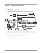
2-2 DC Power Distribution: DC Regulation and Distribution
When the radio is turned on, SWB+ is present and is applied to:
• transistor switch Q494 (pins 1 and 6) which turns on Q493
• RX audio power amplifier U490
• voltage divider R420/R421 and port PE0, a microprocessor A/D input which measures battery
voltage and radio on/off status
The output of FET switch Q493 is applied to the control pins of regulators U310, U320 and U330,
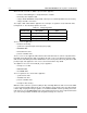
turning them on. The following regulators are used:
The 5 V source is applied to:
• RX back end circuitry
• synthesizer super filter input and charge pump supply
• RED/GRN LEDs
• RX audio buffer U510
• portions of ASFIC U451
The 5 V source is also applied to FET switches Q311 and Q312. Q311 is turned on by Q313 when
RX_ENA (from U401 pin 49) is high, and supplies the "5R" source to the RF front end stages Q21-
Q22, and the VCO RX injection buffer Q280. Q312 is turned on by Q313 when TX_ENA (from U401
pin 50) is high, and supplies the "5T" source to the first transmitter stage Q100.
The digital 3.3 volt source from U320 (D_3.3 V) is applied to:
• microprocessor U401
• EEPROM U402
• flash ROM U404
The 3 V regulated source from U330 is applied to:
• synthesizer IC U201
• VCO/buffer IC U251
• portions of ASFIC U451
• microphone bias circuitry
While the radio is turned on, port PH3 (U401 pin 44) is held high. When the radio is turned off, SWB+
is removed and port PE0 (U401 pin 67) goes low, initiating a power-down routine. Port PH3 (pin 44)
remains high, keeping the voltage regulators on via Q493 and Q494, until the operating state of the
radio has been stored in EEPROM and other turn-off data functions have been completed. PH3 then
goes low, turning off Q494 and Q493, and all regulated voltages are removed.
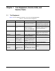
Table 2-1. Voltage Regulators
Reference No. Description Type
U310 5 V Regulator TK71750S
U320 Digital 3.3 V Regulator LP2986
U330 3 V Regulator TK71730S