
Service manual


6880309N62-C June, 2005
136-162 MHz VHF Theory Of Operation: VHF Frequency Generation Circuitry 4-5
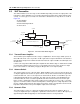
Transmit modulation from the ASFICcmp (U451 pin 40) is applied to U201 pin 10 (MOD_IN). An
electronic attenuator in the ASFICcmp adjusts overall transmitter deviation by varying the audio level
applied to the synthesizer IC. Internally the audio is digitized by the Fractional-N synthesizer and
applied to the loop divider to provide the low-port modulation. The audio is also routed through an
internal attenuator for the purpose of balancing the low port and high port modulation and reducing
the deviation by 6 dB for 12.5 kHz channels, and is available at U201 pin 41 (VCO_MOD). This audio
signal is routed to the VCO's modulator.
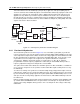
Figure 4-3. VHF Frequency Generation Unit Block Diagram
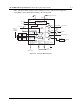
4.4.1 Fractional-N Synthesizer
The Fractional-N synthesizer, shown in Figure 4-4, uses a 16.8 MHz crystal (Y201) to provide the
reference frequency for the system. External components C201-C203, R202 and D201 are also part
of the temperature-compensated oscillator circuit. The dc voltage applied to varactor D201 from U201
pin 25 is determined by a temperature-compensation algorithm within U201, and is specific to each
crystal Y201, based on a unique code assigned to the crystal that identifies its temperature
characteristics. Stability is better than 2.5 ppm over temperatures of -30 to 60 °C. Software-
programmable electronic frequency adjustment is achieved by an internal DAC which provides a
frequency adjustment voltage from U201 pin 25 to varactor D201.
The synthesizer IC U201 further divides the 16.8 MHz signal to 2.1 MHz, 2.225 MHz, or 2.4 MHz for
use as reference frequencies. It also provides a buffered 16.8 MHz signal at U201 pin 19 for use by
the ASFICcmp.
To achieve fast locking of the synthesizer, an internal adapt charge pump provides higher current at
U201 pin 45 to quickly force the synthesizer within lock range. The required frequency is then locked
by the normal mode charge pump at pin 43. A loop filter (C243-C245 and R243-R245) removes noise
and spurs from the steering voltage applied to the VCO varactors, with additional filtering located in
the VCO circuit.
Both the normal and adapt charge pumps get their supply from the capacitive voltage multiplier made
up of C221-C224 and D220-D221. Two 3 V square waves from U201 pins 14-15 provide the drive
signals for the voltage multiplier, which generates 12.1 V at U201 pin 47. This voltage is filtered by
C225-C228.
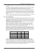
Synthesizer
U201
VCOBIC
U251
Voltage
Multiplier
Loop
Filter
To Mixer
To PA Driver
VCP
Vmult1
Vmult2
Aux3
MOD Out
Modulating
Signal
Rx VCO
Circuit
Tx VCO
Circuit
TRB
16.8 MHz
Ref. Osc.
Rx Out
Tx Out
Buffer
Q280