
Service manual

68P81076C25-C July 1, 2002
Theory of Operation: RF Board 3-5
3.1.2.4 Phase Modulator
ASTRO radios use a dual-port modulation scheme. The nature of the synthesizer loop is to track out
low-frequency errors. In order to enable low-frequency modulation, such as DPL, the reference
signal is modulated with the same signal as the VCO. Effectively, this prevents the low-frequency
error in the loop (DPL) from tracking out because the same error is on the reference signal. The net
effect is that the leading edge of the reference pulse is time-varying at the same rate as the loop
pulse; therefore, there is no phase error between the two signals and low-frequency modulation is
allowed to pass.
The phase modulation comparator has two inputs: U602, pins 28 and 29. R625 and C630 form an
exponential ramp into the plus side of the comparator on U602, pin 29. This ramp is tickled at the
reference rate. R626 and C631 form an integrator through which modulation is applied to the minus
side of the comparator. The comparator trips when the ramp voltage reaches the voltage on U602,
pin 28. The output of the comparator is the time-shifted leading edge of F
r
.
3.1.2.5 Loop Filter
ASTRO radios use a switchable, dual-bandwidth loop filter. They also use adaptive filter switching to
achieve fast lock. The output of the phase detector is routed to an external device (Q608), the output
of which is routed back into the IC for proper filter path selection.
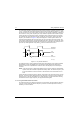
In normal operation, the high drive buffer output is routed through the appropriate transmission gates
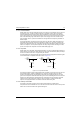
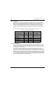
into the selected filter. A simplified schematic is shown in Figure 3-4.
Figure 3-4. Loop Filter Schematic
The loop filters greatly minimize voltage transients that contribute to system hum and noise but, due
to their lowpass nature, it takes considerable time to change the average charge in the filters.
Therefore, the adapt scheme was implemented. When the radio is changing frequency, the loop
goes into the adapt mode. Selected transmission gates in the IC effectively place a short across the
resistors in the filter (eliminating associated RC time constants) and quickly charge the loop filter
capacitors to the correct steering line voltage for the new frequency. At the end of the adapt
sequence, the appropriate filter is reconnected via internal transmission gates.
3.1.2.6 Auxiliary Control Bits
The auxiliary control bits are system control outputs whose states are controlled by the
microprocessor via the serial data bus. AUX 1 and AUX 2 are sent to the first VCO to control pin shift
states. AUX 3 controls the state of the negative steering line.
IN
OUT
R615
NARROW BAND WIDE BAND
IN OUT
R616 R617
C626 C654 C625 R614
R613 C625
C623
C623
MAEPF-25184-O