
Computer Accessories User Manual

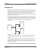


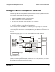

Devices’ Features and Data Paths FPGA
116 PENT/ATCA−717
compliant to the IPMI specification V1.5 Rev. 1.0 and share one Interrupt Source register.
The first BT interface is used as the only System Interface and uses IPMI channel 0x0F.
The second BT interface uses IPMI channel 0x06.
aaa
Port 80 Register
The FPGA provides an 8−bit wide register to store POST codes. The register is located at
I/O address 80
16
.. It is only readable for the IPMC and read−writeable for the host. The
IPMC polls this register to monitor the boot up sequence of the board. The content of the
port 80 register can also be obtained and read via IPMI.
a
IPMC Extensions
The FPGA implements three registers which are only visible for the IPMC. These registers
reflect the following:
S CPU core voltage identifier
S Frame signal on LPC bus
S System and parity errors on PCI buses
S Enabling/disabling of backplane signals used for electronic keying
S Alert signals
Clock Synchronization Extensions
The FPGA contains extensions which are related to the AdvancedTCA clock
synchronization feature. These extensions include:
S Registers accessible via host and IPMC for controlling and monitoring clock
synchronization
S SPI interface for controlling DPLL device
S Programmable clock divider
a
For further details refer toasection "Clock Synchronization Interface" on pagea124a
andasection "Clock Synchronization Interface Registers" on pagea144.
Reset Controller
The FPGA contains part of the blade′s reset logic. Furthermore it provides two registers
which allow to determine the source of the last reset issued and to mask resets.
a
Reset Types
Two different types of resets are possible: hard resets and soft resets.
a