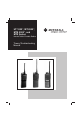
HT 1000™, MT 2000™, MTS 2000™, and MTX Series Handie-Talkie® Portable Radios Theory/Troubleshooting Manual
HT 1000TM, MT 2000TM, MTS 2000TM, and MTX Series Handie-Talkie® Portable Radios Theory/Troubleshooting Manual *6881200C15* 68P81200C15-O Motorola 8000 West Sunrise Boulevard Fort Lauderdale, Florida 33322
Foreword The information contained in this manual relates to all HT 1000™, MT 2000™, MTS 2000™, and MTX Series Handie-Talkie® portable radios, unless otherwise specified. For details on the operation of the radio, refer to the applicable manuals, which are available separately. A list of related publications is provided in the section, “Related Publications Available Separately” on page iii.
HT 1000TM, MT 2000TM, MTS 2000TM, and MTX Series Handie-Talkie® Portable Radios CONTENTS TITLE PAGE LIST OF TABLES...................................................................................................................................................iii LIST OF FIGURES.................................................................................................................................................iii RELATED PUBLICATIONS AVAILABLE SEPARATELY ......................................
CONTENTS (cont.) TITLE PAGE THEORY OF OPERATION (DETAILED FUNCTIONAL DESCRIPTION) I. INTRODUCTION ...........................................................................................................................................10 II. RADIO POWER .............................................................................................................................................10 A. General....................................................................................................
LIST OF TABLES TABLE 1 2 3 TITLE PAGE Option Select Definition...........................................................................................................18 Option Select Definition...........................................................................................................29 Universal Connector Mode......................................................................................................
GLOSSARY OF TERMS ALC- Automatic Level Control; a circuit in the transmit RF path that controls RF power amplifier output, provides leveling over frequency and voltage, and protects against high VSWR ASF IC- Audio Signalling Filter Integrated Circuit Closed architecture- A controller configuration that utilizes a microcomputer with internal ROM, RAM, and EEPROM DTMF- Dual Tone Multi-frequency DPL- Digital Private-Line™ Firmware- Software or a software/hardware combination of computer programs and data, with
INTRODUCTION I. PURPOSE This manual will provide a theoretical explanation of the HT 1000, MT 2000, MTS 2000, and MTX Series portable radio’s operation, troubleshooting, and additional useful information about the radio not found in any other publication. The manual is divided into three sections: • • • INTRODUCTION THEORY OF OPERATION TROUBLESHOOTING In the THEORY OF OPERATION section, a basic functional description is followed with a more detailed description of some selected circuits.
THEORY OF OPERATION (BASIC FUNCTIONAL DESCRIPTION) I. INTRODUCTION This publication covers a large family of portable radios: HT 1000, MT 2000, MTS 2000, and MTX series units. They are software driven, and because of the wide range of operating systems and radio functionality provided by this family of radios, the theory discussions will be divided into several major categories. The transceiver is frequency sensitive and falls into one of four frequency bands: vhf, uhf, 800MHz, or 900MHz.
SB+ U709 U706 5V Regulator Audio PA SB+ On 5V Off B+ 5V U701 U705 Micro C Controls Flex ASF IC B+ Controller Board SB+ Front Cover Flex Opt B+ Universal Connector SB+ Jumper Flex Raw B+ SB+ Fuse 1 Amp Harmonic Filter U101 L105 CR109 CR108 Vcc L122 L121 SB+ PA Module ALC RX RF Amp + Battery 7.5V U105 T5 5V Regulator VCOB IC U201 U202 5V T5 Mixer Q107 R5 Q105 S Out R/T 5V Ref Osc Synth U103 5V Regulator IF IC D/A IC Transceiver Board Figure 1A.
In the transceiver, SWB+ is routed directly to the 5v regulator (U202). The regulated 5v supplies the IF IC (U3), the reference oscillator (U203), the Fractional-N synthesizer IC (U204), the D/A IC (U102), and the R/T switch (Q108). VCO buffer signal is applied to a comparator in the synthesizer. The synthesizer comparator also receives a reference frequency via a reference divider input from the 16.8 MHz temperature-compensated reference oscillator.
The filtered RF signal is then applied to the RF input of a broadband mixer IC. An injection signal (FIRST LO), supplied by the FGU, is applied to the second input of the mixer stage. The resulting difference frequency (44.85MHz for VHF and 73.35MHz for UHF), is the first IF frequency. The first IF frequency is then filtered by a 2-pole crystal filter to remove unwanted mixer products and routed to the IF IC. is replaced by internal filters in the IF IC.
The RF PA module is a multi-stage amplifier, which has the required gain to produce an output level of several watts. Some harmonic filtering is accomplished in the RF PA. IV. 800/900MHz TRANSCEIVER BOARD Modulation of the carrier is achieved by using a 2port modulation technique. The deviation of the low frequency tone, such as DPL/TPL, is achieved by injecting the signal to an analog/digital circuit in the synthesizer.
D. Receiver Back End (See Figure 6) E. Transmitter (See Figure 7) In the IF IC, the first IF frequency is down converted, amplified, filtered, and demodulated to produce the recovered audio. The IF IC is electronically programmable, and the amount of filtering, which is dependent on the radio channel spacing, is controlled by the microprocessor. Filtering is accomplished by internal filters in the IF IC.
overall PA gain as appropriate. Another function of the detector is to provide a signal when the VSWR exceeds the threshold level. This signal, combined with the forward detected power, is used to reduce the PA output power, thus protecting the PA under high VSWR conditions. V. CLOSED ARCHITECTURE CONTROLLER A. General (See Figure 8) The controller board is the central interface between various subsystems of the radio. It is segregated into digital and audio architecture.
External Microphone Internal Microphone 2.1/2.4 MHz REF Clock From FGU Squelch Expander External Speaker U702 Audio PA Compressor Recovered Audio Internal Speaker U701 ASF IC Flutter Filter Audio/ Signalling Architecture *U601 HEAR/CLEAR Mod Out To FGU SPI To Receiver Board uP Clock U710 SLIC Masked ROM or FLASH U705 MCII FI u Processor SCI To Universal Connector EEPROM SRAM Digital Architecture MAEPF-23422-O * U601 HEAR/CLEAR used on 900 MHz radios only. Figure 9.
THEORY OF OPERATION (DETAILED FUNCTIONAL DESCRIPTION) I. INTRODUCTION In this section of the of the manual, a more detailed description of the radio and some special circuit is given. For a better understanding of the circuits descriptions, and to aid in following the text, refer to the applicable schematic diagram(s) in the corresponding service manual (Motorola part number 68P81200C25), or previously 68P81200C20. II. RADIO POWER A.
The OPT B+ voltage powers external accessories used with the radio. C. B+ Routing and DC Voltage Distribution (for an Open Architecture Controller and an 800 or 900MHz Transceiver) This radio differs from previous Motorola portable radios in that B+ from the battery is electrically switched to most of the radio, rather than routed through the on/off/volume switch, S403/R401. The electrical switching of B+ supports a ”keep-alive” mode.
The open architecture controller board uses Flash memory (U715) in place of conventional EPROMs. This allows the firmware to be reprogrammed through the side connector without opening the radio. The smart RIB box (SRIB) is used in conjunction with the RSS software program to perform the Flash reprogramming operation. While this occurs, the SRIB applies 12.7 V at different times to two of the radio side connector pins, 4 and 10. Pin 4 is the OPT B+/BOOT SEL pin. When 12.
C80, C86, C87, C88, C97, C99, L3, L4, L5, and L30 (VHF); or C4 thru C7, C88 thru C94, C99, and L11 thru L15 (UHF) to improve the spurious rejection. Via a broadband 50-ohm transformer, T1, the filtered RF signal is routed to the input of a broadband mixer/buffer (U2). Mixer U2 uses GaAs FETs, in a double-balanced Gilbert Cell configuration. The RF signal is applied to the mixer at U2 pins 1 and 15. An injection signal (1st LO) of about -10dBm, supplied by the FGU, is applied to U2 pin 8.
3. ALC Circuits Coupler module U104 samples the forward power and the reverse power of the PA output voltage. Reverse power is present when there is other than 50 ohms impedance at the antenna port. Sampling is achieved by coupling some of the forward and/or reverse power, and apply it to CR102(VHF) or CR101(UHF) and CR103 for rectification and summing. The resultant dc signal is then applied to the TX ALC IC (U101 pin 2) as RFDET to be used as an RF strength indicator.
the SRL. The loop divider adds or subtracts phase to the prescaler divider by changing the divide ratio via the modulus control line. The output of the prescaler is then applied to the loop divider. The output of the loop divider is then applied to the phase detector. The phase detector will then compare the loop divider’s output signal with the signal from U203 (that is divided down after it is applied to pin 14 of U204).
The final stage in the receiver front end is a 2-pole crystal filter, FL12. The crystal filter provides some of the receiver’s adjacent channel selectivity. The receiver’s backend IF IC (U3) provides most of the adjacent channel selectivity, using integrated baseband low-pass filters. The input to the crystal filter is matched to the 1st mixer using components L36, L20, C35 and C36. The output of the crystal filter is matched to pin 2 of the IF IC using inductor L22, and a capacitive tap C38 and C39. D.
2. Microcomputer Clock Synthesizer Upon power-up, and assuming that the ASF IC receives a proper 2.1MHz input at U701 pin 33 (which comes from the transceiver board), the ASF IC outputs a 3.6864MHz CMOS square wave on U701 pin 35. This UP CLK signal connects to the input of the microcomputer (U705 pin 77) as EXTAL. The microcomputer operates at 1/4 of this frequency, which in this case computes to 921.6KHz.
dual NPN transistor IC, U704. When either of the outputs (U705 pin 66, PC1 or U705 pin 65, PC0) is at a logic high, the corresponding output of U704 (pin 3 for the green LED, pin 6 for the red ) is at approximately 4.3volts. Note that it is possible to have both LED outputs on simultaneously, in which case the LED emits an orange/yellow light. blocking components. The high-pass filter formed by capacitor C779 and resistor R704 attenuates objectionable low-frequency audio components of speech.
a. Sub-audible Data (PL/DPL) Sub-audible data is composed of low-frequency PL and DPL waveforms for conventional operation. Although it is referred to as “sub-audible data,” the actual frequency spectrum of these waveforms may be as high as 250 Hz, which is audible to the human ear. However, the radio receiver filters out any audio below 300 Hz, so these tones are never heard in the actual system. Only one type of sub-audible data can be generated by U705 at any one time. The process is as follows.
U705 pin 51, PE1. After passing through the 8bit digital attenuator, the audio goes to a buffer amplifier and exits the module at U701 pin 21 (RX AUD OUT), where it is routed to audio PA module U706 (pin 8). and routing the signal to a comparator, which outputs a logic zero or a logic one signal. The discriminator output from the transceiver board is routed to U701 pin 15 through coupling capacitor C710.
the external memory devices, U705 has 1k of RAM and 512 bytes of EEPROM on chip. Miscellaneous logic and switching functions are provided by U703, U709, and U711. Since the controller is the central interface between the various subsystems of the radio, and because of the controllers complexity, this section will be divided into two areas of discussion, the microcomputer and its associated circuits, and the controller board’s circuit operation. A. Microprocessor (U705) and Associated Circuits 1.
common symptom is the RESET line goes low periodically, with the period being on the order of msec. 5. RAM The on-chip 1k static RAM from U705 provides some scratch-pad memory, with the bulk of it coming from the external 32K SRAM U714. External SRAM accesses are indicated by the CSGEN signal U714 pin 20 (which comes from U705-PG6) going low. Normally RAM is accessed less often than the Flash U715; i.e.
(J701 pin 9) to go low. The multiprocessor detects this transition using U710, and then sends a command to the display in order to read the keypad data. The secure/data option board, which connects to connector jack J702, supports two slave SPI devices, which can each return data to the multiprocessor. The connector pins for these devices are J702 pins 21 and 23, and the interrupt lines (which performs the same function as the KEY INT line above) J702 pins 20 and 22.
Although it is referred to as “sub-audible data,” the actual frequency spectrum of these waveforms may be as high as 250Hz, which is audible to the human ear. However, the radio receiver filters out any audio below 300Hz, so these tones are never heard in the actual system. Only one type of sub-audible data can be generated by U701 at any one time.
secure board it is decrypted and converted back to analog format, and then fed back to the ASF IC from the AUX RX line (J702 pin 9). It is then routed to the ASF IC pin U701-J6; from then on it traverses a path identical to conventional receive audio 4. Receive Data Circuits The ASF IC (U701) decodes all receive data, which includes PL, DPL, low-speed trunking, MDC, and high-speed trunking data.
Pin 10, the Vpp/CTS pin, also serves several functions. When reprogramming the Flash memory device, this pin carries the programming voltage, Vpp. The pin is also used to identify that a key-variable loader is attached. The KVL cable will ground this pin. Pin 11, the BOOT PGM RX/TX DATA pin, is used for receive data during bootstrap programming, typically when reprogramming the Flash. Unlike normal SB9600 communications, bootstrap mode requires separate receive and transmit data paths.
TROUBLESHOOTING I. INTRODUCTION A. Check Batteries Servicing the HT 1000, MT 2000, MTS 2000, and MTX series portable radios requires the localization of the malfunctioning circuit before the defective component can be isolated and replaced. Since localizing and isolating a defective component constitutes the most time consuming part of troubleshooting, a thorough understanding of the circuits involved will aid the technician in performing efficient servicing.
D. Check Overall Receiver Operation 1. 20dB Quieting Sensitivity Test A good overall check of receiver operation is the 20dB quieting sensitivity measurement. This check will indicate that the receiver has sufficient gain and that all of the included circuitry is working properly. The quieting signal is that rf signal input necessary to reduce the audio output at the speaker by 20dB. This measurement should be made with no modulation.
TROUBLESHOOTING FLOW CHART (VHF/UHF Transceiver/Closed Architecture Controller) Start * Note: Assumes Power Beep is Enabled Good Power Up Beep?* NO Radio Drawing NO Stand-by Current About 60mA? YES Is There TX Power? NO Go to Transmitter Chart #1A Is TX Deviation OK? NO Go to No Transmit Deviation Chart #7A Press Monitor Audio Noise? NO Go to No Receiver Audio Chart #6A Good SINAD? NO Is R5 on? YES NO NO Go to Controller Chart #8A End MAEPF-23279-O 32 Go to Controller Chart #8A NO
TROUBLESHOOTING FLOW CHART (800/900MHz Transceiver/Open Architecture Controller) Start * Note: Assumes Power Beep is Enabled Good Power Up Beep?* NO Radio Drawing NO Stand-by Current About 60mA? YES Is There TX Power? NO Go to Transmitter Chart #1B Is TX Deviation OK? NO Go to No Receiver Audio Chart #6B Press Monitor Audio Noise? No Receive Audio? Poor SINAD? Go to Controller Chart #8B NO YES Go to No Receiver Audio Chart #6B YES Is RS on? YES NO Radio Decoding? Check Fuse, Volume S
TROUBLESHOOTING FLOW CHART #1A (VHF/UHF Transmitter RF) No/Low Power TX Current > 500 mA? Replace RF Jack, S101 YES NO Is T5 On at C153? YES YES RF at RF Jack, S101 Pin 3? B+ at U105, Pin 5 (VHF) 5,6 (UHF)? NO Check Components Between C147 and L128 YES YES 7.5V at U105 Pin 2,4? 2.
TROUBLESHOOTING FLOW CHART #1B (800/900MHz Transmitter RF) Replace Ant Contact No/Low Power BAD TECHNICAL PUB Check GOOD Continuity at Ant. Cont.
TROUBLESHOOTING FLOW CHART #2A (VHF/UHF Receiver RF) Bad SINAD Bad 20Db Quieting No Recovered Audio NOTE: INJECT MODULATED ON CARRIER FREQUENCY SIGNAL AS REQUIRED YES YES Audio at C306? Check Controller NO Spray or Inject 1st IF into XTAL Filter IF FREQS: 44.85 VHF 73.35 UHF YES Inject RF into J401 NO Audio Heard? Check 2nd LO Cntrl Voltage at R16 IF Signal at L20? YES YES NO RF Signal at T1? VCO Locked? 2.1/2.
TROUBLESHOOTING FLOW CHART #2B (800/900MHz Receiver RF) No-High SINAD Inject 73.350MHz at Pin 1 FL1 -110 = 12dB SINAD NO Check Freq. Pin 14-U3 NO VDC at Pin 18 U3 0 or 5V YES Check Comp. Q1, CR5, C54, C55, L24, C56 & C57 YES YES NO Check U3 & Ext. Comp. Inject 73.350MHz at L20/C35 -113-12dB SINAD NO YES Inject Carrier at Pin 2 of U5 12dB SINAD -108dBm NO YES Replace U5 NO Check Comp.
TROUBLESHOOTING FLOW CHART #3A (VHF/UHF DC Switch) No R5 Q105 Pin 2 YES Voltage at Q105 Pin 3? NO Replace Q105 Voltage at U103, Pin 3? YES Less than 4.8V at Q105 Pin 1? NO Replace U102 YES NO Voltage at Q107, Pin 2? 5V at U102 Pin 1? YES Voltage at Q107, Pin 3? 7.5V at U202 Pin 8? Voltage at Q107, Pin 4? NO ISS.
TROUBLESHOOTING FLOW CHART #3B (800/900MHz DC Switch) No R5/No T5 YES Voltage at Q108, Pin 4? NO 0V at Q108: Pin 5 - RX Pin 3 - TX Voltage at U202 Pin 1? YES Check Continuity Between U202-1 & Q108-4 NO YES Check U102 VDC U202-8 YES Replace U202 NO VDC J301-2 NO Check Jumper Flex YES VDC U712-2 YES VDC U712-4 LOW = ON NO VDC Q703-1 HIGH = ON NO VDC J703-10 NO VDC J703-8 Replace P404 YES NO Replace U712 VDC P404-1 NO YES Replace Q703 YES YES Replace Control Flex Replace CR70
NO VDC at U204 Pin 21, 28(Tx), 29(Rx) 37 & 38 OK? Replace U202 Go to VCO TX/RX Unlock Troubleshooting Chart #5A 16.8 MHz at U204 Pin 14? YES YES YES VDC at CR205 Pin 4 OK? NO YES NO 2.5V at U204 Pin 7 & 8? JWB 3/31/93 SW 3/31/93 ) RLSE. O ISS. REVISION RLSE. ) ( O.K. AS MARKED ( CORRECTED AS MARKED DATE 3/31/93 EDITOR JWB CHECKER 12/16/92 SW LETTERING SIZE: REQUIRES: DATE Illustrator O.K. AS IS DISK C63 PROGRAM DATE 16.8 MHz at U203 Pin 10? YES NO 2.
TROUBLESHOOTING FLOW CHART #4B (800/900MHz Frequency Generation Unit - FGU) FGU No Lo Injection/TX Unlock A VDC at V Con Pin 1 U205 <0.7V ? NO 5V at U204 Pin 11, 20, 23, 25, 42? YES ILLUSTRATOR DATE SW 3/12/93 EDITOR DATE JWB 3/22/93 ENGINEER DATE CHECKER DATE LETTERING SIZE: REQUIRES: PROGRAM DISK Illustrator C68 CHECK ONE ISS. O ( ) O.K. AS MARKED ( ) O.K. AS IS CORRECTED AS MARKED REVISION RLSE. RLSE.
TROUBLESHOOTING FLOW CHART #5A (VHF/UHF Voltage Controlled Oscillator - VCO) VCO TX/RX UNLOCK Check VDC at C246 (VCTRL) Replace U201 NO VDC 13V/0.7V/ Drifting ? RX ONLY * NOTE: If C240 is found defective, change to 2.7PF (VHF)/ 2.4PF (UHF1)/2.4PF (UHF2) TX ONLY * NOTE: If C240 is found defective, change to 2.7PF (VHF)/ 2.4PF (UHF1)/2.4PF (UHF2) YES For VHF check L217. If OK replace U201. NO 4.6V at Collector of Q202? Replace components & go to -VEE crossover freq. tune procedures.
TROUBLESHOOTING FLOW CHART #5B (800/900MHz Voltage Controlled Oscillator - VCO) VCO TX/RX Unlock VDC U205-9 VDC U204-19 NO YES NO YES 5VDC U205-8 850-870MHz 935-941MHz YES NO NO 5VDC U201-6 806-825MHz 896-902MHz YES NO YES NO Check Continuity Between U204-19 & U205-9 5VDC U205-3 777-825MHz 862-902MHz VDC U204-20 NO Refer to Chart #3B DC YES Measure Freq. U201-15 Check C253 if OK Change U204 YES NO VDC U205-1, 7 VDC U204-17 Measure Freq.
TROUBLESHOOTING FLOW CHART #6A (VHF/UHF, Closed Architecture, No Receive Audio) NO DISK MAEPF-23275 PROGRAM TECHNICAL PUBLICATIONS DEPT. DWG. NO. DATE Replace U709 DESCRIPTION ENGINEER YES RLSE. ) CHECK ONE ) RLSE. 7.5V at U709, Pin 8? ( O.K. AS IS O.K. AS MARKED ( NO SW JWB 3/31/93 3/31/93 Audio at U706 Pin 4, Pin 2 NO 5V at U709, Pin 1? C63 REVISION NO ILLUS. NO CORRECTED AS MARKED Check Control Top Flex, P403 RF Controller Flex P301, VOl SW. O YES Check Spk.
TROUBLESHOOTING FLOW CHART #6B (800/900MHz, Open Architecture, No Receive Audio) No/Low Audio Inject on Freq.
TROUBLESHOOTING FLOW CHART #7A (VHF/UHF, Closed Architecture, No Transmit Deviation) Check Continuity between V Gnd MK401 = 2k NO Acoustic Couple 1k tone to Int. Mic. NO Check Audio at Pin 2-U701 NO Check Components R701, L710, R703, C779, & C706 MBEPF-23276-O NO YES INT VDC at MK401 and Gnd. No TX Deviation EXT NO Setup: Injects 80mV: 1kHz sinusoidal tone into Ext.
TROUBLESHOOTING FLOW CHART #7B (800/900MHz, Open Architecture, No Transmit Deviation) No TX Dev. Ext. Setup - Inject 80mV-1k Signal into Ext. Mic. Path INT NO VDC at MK401 and Gnd YES Check Audio 14-J701 NO Check Continuity between Pin 14-J701 & Pin 3 J403 NO Check Components R703, R704, C712 YES Acoustic Couple 1k Tone to Int. Mic.
TROUBLESHOOTING FLOW CHART #8A (Closed Architecture Controller) PTT EMER Press PTT. Red LED does not light up. Enable and press EMER. Button. Red LED does not blink. NO PTT OK? YES Press EMER Button U705 pin 62 low? Press MON. Button, Radio does not respond. Press PTT, U705 Pin 61 Low? See PTT Troubleshooting NO Press MON Button U705 pin 59 low ? Check U703-1 Voltage PTT SW YES PTT J704-4 HIGH? YES Check J703-18 Voltage. EMER.
Motorola, Inc. 8000 West Sunrise Boulevard Ft. Lauderdale, FL 33322 MOTOROLA and the Stylized M Logo are registered in the U.S. Patent and Trademark Office. All other product or service names are the property of their respective owners. © Motorola, Inc. 2003. All rights reserved. Printed in U.S.A.