
user manual


Connectors and Jumper Settings
http://www.motorola.com/computer/literature 2-15
2
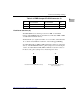
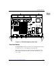
Flash Bank Selection (J6)
The CPX750HA base board has provision for 1MB of 16-bit flash
memory. The RAM300 memory mezzanine accommodates 4MB or 8MB
of additional 64-bit flash memory.
The flash memory is organized in either one or two banks, each bank either
16- or 64-bits wide. Bank B contains the onboard debugger, PPCBug.
To enable flash bank A (4MB or 8MB of firmware resident on soldered-in
devices on the RAM300 mezzanine), place a jumper across header J6 pins
1 and 2. To enable flash bank B (1MB of firmware located in sockets on
the base board), place a jumper across header J6 pins 2 and 3.
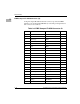
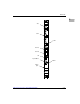
45 NO CONNECT NO CONNECT 46
47 DATA8 DATA9 48
49 DATA10 GND 50
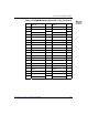
Table 2-8. EIDE Compact FLASH Connector J9
3
2
1
3
2
1
Flash Bank A Enabled (4MB/8MB, Soldered) Flash Bank B Enabled (1MB, Sockets)
J6J6
(Factory Configuration)