
user manual

PLL OPERATION CONSIDERATIONS
MOTOROLA
PLL CLOCK OSCILLATOR 9 - 11
9.4 PLL OPERATION CONSIDERATIONS
The following paragraphs discuss PLL operation considerations.
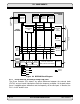
9.4.1 Operating Frequency
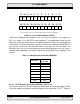
The operating frequency of the chip is governed by the frequency control bits in the PLL
control register as follows:
where: DF is the division factor defined by the DF0-DF3 bits
F
CHIP
is the chip operating frequency
F
EXT
is the external input frequency to the chip at the EXTAL pin
F
VCO
is the output frequency of the VCO
MF is the multiplication factor defined by the MF0-MF11 bits
The chip frequency is derived from the output of the low power divider. If the
low power divider is bypassed, the equation is the same but the division factor
should be assumed to be equal to one.
9.4.2 Hardware Reset
Hardware reset causes the initialization of the PLL. The following considerations apply:
1. The MF0-MF11 bits in the PCTL register are set to their pre-determined hard-
ware reset value. The DF0-DF3 bits and the Chip Clock Source bit in the
PCTL register are cleared. This causes the chip clock frequency to be equal to
the external input frequency (EXTAL) multiplied by the multiplication factor
defined by MF0-MF11.
2. During hardware reset assertion, the PINIT pin value is written into the PEN
bit in the PCTL register. If the PINIT pin is asserted (setting PEN), the PLL
acquires the proper phase/frequency. While hardware reset is asserted, the
internal chip clock will be driven by the EXTAL pin until the PLL achieves lock
(if enabled). If the PINIT pin is deasserted during hardware reset assertion, the
PEN bit is cleared, the PLL is deactivated and the internal chip clock is driven
by the EXTAL pin.
3. PLOCK is a reliable indicator of the PLL lock state only after exiting the hard-
ware reset state.
F
CHIP
F
EXT
MF×
DF
---------------------------
Fvco
DF
--------------==