MOTOROLA SEMICONDUCTOR Order this document by MC68HC912B32TS/D TECHNICAL DATA MC68HC912B32 Technical Summary 16-Bit Microcontroller 1 Introduction The MC68HC912B32 microcontroller unit (MCU) is a 16-bit device composed of standard on-chip peripherals including a 16-bit central processing unit (CPU12), 32-Kbyte flash EEPROM, 1-Kbyte RAM, 768-byte EEPROM, an asynchronous serial communications interface (SCI), a serial peripheral interface (SPI), an 8-channel timer and 16-bit pulse accumulator, an 8-bit
— Programmable Center-Aligned or Left-Aligned Outputs • Serial Interfaces — Asynchronous Serial Communications Interface (SCI) — Synchronous Serial Peripheral Interface (SPI) — J1850 Byte Data Link Communication (BDLC) • COP Watchdog Timer, Clock Monitor, and Periodic Interrupt Timer • 80-Pin QFP Package — Up to 63 General-Purpose I/O Lines — 2.7V–5.5V Operation at 8 MHz • Single-Wire Background Debug™ Mode (BDM) • On-Chip Hardware Breakpoints 1.
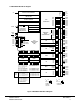
TABLE OF CONTENTS Section 1 Page Introduction 1.1 1.2 1.3 2 1 Features ......................................................................................................................................1 Ordering Information ...................................................................................................................2 MC68HC912B32 Block Diagram .................................................................................................5 Central Processing Unit 2.1 2.2 2.
TABLE OF CONTENTS (Continued) Section 11 Page Pulse-Width Modulator 11.1 11.2 12 12.1 12.2 13 13.1 13.2 13.3 13.4 14 14.1 14.2 14.3 14.4 14.5 15 15.1 15.2 15.3 16 16.1 16.2 16.3 16.4 63 PWM Register Description ........................................................................................................65 PWM Boundary Cases ..............................................................................................................72 Standard Timer Module 73 Timer Registers ...........
1.
2 Central Processing Unit The CPU12 is a high-speed, 16-bit processing unit. It has full 16-bit data paths and wider internal registers (up to 20 bits) for high-speed extended math instructions. The instruction set is a proper superset of the M68HC11instruction set. The CPU12 allows instructions with odd byte counts, including many single-byte instructions. This provides efficient use of ROM space.
2.2 Data Types The CPU12 supports the following data types: • Bit data • 8-bit and 16-bit signed and unsigned integers • 16-bit unsigned fractions • 16-bit addresses A byte is eight bits wide and can be accessed at any byte location. A word is composed of two consecutive bytes with the most significant byte at the lower value address. There are no special requirements for alignment of instructions or operands. 2.
2.4 Indexed Addressing Modes The CPU12 indexed modes reduce execution time and eliminate code size penalties for using the Y index register. CPU12 indexed addressing uses a postbyte plus zero, one, or two extension bytes after the instruction opcode.
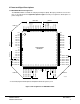
3 Pinout and Signal Descriptions 3.1 MC68HC912B32 Pin Assignments The MC68HC912B32 is available in a 80-pin quad flat pack (QFP). Most pins perform two or more functions, as described in the 3.3 Signal Descriptions. Figure 3 shows pin assignments. Shaded pins are power and ground.
3.2 Power Supply Pins MC68HC912B32 power and ground pins are described below and summarized in Table 4. 3.2.1 Internal Power (VDD) and Ground (VSS) Power is supplied to the MCU through VDD and VSS. Because fast signal transitions place high, shortduration current demands on the power supply, use bypass capacitors with high-frequency characteristics and place them as close to the MCU as possible. Bypass requirements depend on how heavily the MCU pins are loaded. 3.2.
3.3 Signal Descriptions 3.3.1 Crystal Driver and External Clock Input (XTAL, EXTAL) These pins provide the interface for either a crystal or a CMOS compatible clock to control the internal clock generator circuitry. Out of reset the frequency applied to EXTAL is twice the desired E-clock rate. All the device clocks are derived from the EXTAL input frequency.
3.3.3 Reset (RESET) An active low bidirectional control signal, RESET, acts as an input to initialize the MCU to a known startup state. It also acts as an open-drain output to indicate that an internal failure has been detected in either the clock monitor or COP watchdog circuit. The MCU goes into reset asynchronously and comes out of reset synchronously. This allows the part to reach a proper reset state even if the clocks have failed, while allowing synchronized operation when starting out of reset.
3.3.8 External Address and Data Buses (ADDR[15:0] and DATA[15:0]) External bus pins share function with general-purpose I/O ports A and B. In single-chip operating modes, the pins can be used for I/O; in expanded modes, the pins are used for the external buses. In expanded wide mode, ports A and B are used for multiplexed 16-bit data and address buses. PA[7:0] correspond to ADDR[15:8]/DATA[15:8]; PB[7:0] correspond to ADDR[7:0]/DATA[7:0].
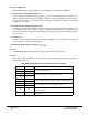
Table 5 MC68HC912B32 Signal Description Summary Pin Name Pin Number Description PW[3:0] 3–6 ADDR[7:0] DATA[7:0] 25–18 ADDR[15:8] DATA[15:8] 46–39 IOC[7:0] 16–12, 9–7 PAI 16 AN[7:0] 58–51 DBE 26 MODB, MODA 27, 28 IPIPE1, IPIPE0 27, 28 ECLK 29 E-clock is the output connection for the external bus clock. ECLK is used as a timing reference and for address demultiplexing.
3.4 Port Signals The MC68HC912B32 incorporates eight ports which are used to control and access the various device subsystems. When not used for these purposes, port pins may be used for general-purpose I/O. In addition to the pins described below, each port consists of a data register which can be read and written at any time, and, with the exception of port AD and PE[1:0], a data direction register which controls the direction of each pin. After reset all port pins are configured as input. 3.4.
When the PUPE bit in the PUCR register is set, PE[7,3,2,0] are pulled up. PE[7,3,2,0] are pulled up active devices, while PE1 is always pulled up by means of an internal resistor. Neither port E nor DDRE is in the map in peripheral mode; neither is in the internal map in expanded modes with EME set. Setting the RDPE bit in register RDRIV causes all port E outputs to have reduced drive level. RDRIV can be written once after reset. RDRIV is not in the address map in peripheral mode.
Register DDRT determines pin direction of port T when used for general-purpose I/O. When DDRT bits are set, the corresponding pin is configured for output. On reset the DDRT bits are cleared and the corresponding pin is configured for input. When the PUPT bit in the TMSK2 register is set, all input pins are pulled up internally by an active pullup device. Pull-ups are disabled after reset. Setting the RDPT bit in the TMSK2 register configures all port T outputs to have reduced drive levels.
Table 6 MC68HC912B32 Port Description Summary Pin Numbers Data Direction DD Register (Address) Port A PA[7:0] 46–39 In/Out DDRA ($0002) Port B PB[7:0] 25–18 Port AD PAD[7:0] 58–51 In Port DLC PDLC[6:0] 70–76 In/Out DDRDLC ($00FF) Port E PE[7:0] 26–29, 35–38 PE[1:0] In PE[7:2] In/Out DDRE ($0009) Mode selection, bus control signals and interrupt service request signals; or general-purpose I/O. Port P PP[7:0] 79, 80, 1–6 In/Out DDRP ($0057) General-purpose I/O.
3.5 Port Pull-Up, Pull-Down and Reduced Drive MCU ports can be configured for internal pull-up. To reduce power consumption and RFI, the pin output drivers can be configured to operate at a reduced drive level. Reduced drive causes a slight increase in transition time depending on loading and should be used only for ports which have a light loading. Table 7 summarizes the port pull-up default status and controls.
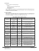
4 Register Block The register block can be mapped to any 2-Kbyte boundary within the standard 64-Kbyte address space by manipulating bits REG[15:11] in the INITRG register. INITRG establishes the upper five bits of the register block’s 16-bit address. The register block occupies the first 512 bytes of the 2-Kbyte block. Default addressing (after reset) is indicated in the table below. For additional information refer to 5 Operating Modes and Resource Mapping.
Table 8 MC68HC912B32 Register Map (Sheet 2 of 5) Address Bit 7 6 5 4 3 2 1 Bit 0 Name $0023 Bit 7 6 5 4 3 2 1 Bit 0 BRKAL $0024 Bit 15 14 13 12 11 10 9 Bit 8 BRKDH $0025 Bit 7 6 5 4 3 2 1 Bit 0 BRKDL $0026– $003F 0 0 0 0 0 0 0 0 Reserved $0040 CON23 CON01 PCKA2 PCKA1 PCKA0 PCKB2 PCKB1 PCKB0 PWCLK $0041 PCLK3 PCLK2 PCLK1 PCLK0 PPOL3 PPOL2 PPOL1 PPOL0 PWPOL $0042 0 0 0 0 PWEN3 PWEN2 PWEN1 PWEN0 PWEN $0043 Bit 7 6 5 4 3 2 1
Table 8 MC68HC912B32 Register Map (Sheet 3 of 5) Address Bit 7 6 5 4 3 2 1 Bit 0 Name $006F PAD7 PAD6 PAD5 PAD4 PAD3 PAD2 PAD1 PAD0 PORTAD $0070 Bit 7 6 5 4 3 2 1 Bit 0 ADR0H $0071 0 0 0 0 0 0 0 0 Reserved $0072 Bit 7 6 5 4 3 2 1 Bit 0 ADR1H $0073 0 0 0 0 0 0 0 0 Reserved $0074 Bit 7 6 5 4 3 2 1 Bit 0 ADR2H $0075 0 0 0 0 0 0 0 0 Reserved $0076 Bit 7 6 5 4 3 2 1 Bit 0 ADR3H $0077 0 0 0 0 0 0 0 0 Reserved $0078
Table 8 MC68HC912B32 Register Map (Sheet 4 of 5) Address Bit 7 6 5 4 3 2 1 Bit 0 Name $0099 Bit 7 6 5 4 3 2 1 Bit 0 TC4 (L) $009A Bit 15 14 13 12 11 10 9 Bit 8 TC5 (H) $009B Bit 7 6 5 4 3 2 1 Bit 0 TC5 (L) $009C Bit 15 14 13 12 11 10 9 Bit 8 TC6 (H) $009D Bit 7 6 5 4 3 2 1 Bit 0 TC6 (L) $009E Bit 15 14 13 12 11 10 9 Bit 8 TC7 (H) $009F Bit 7 6 5 4 3 2 1 Bit 0 TC7 (L) $00A0 0 PAEN PAMOD PEDGE CLK1 CLK0 PAOVI PAI PACTL $
Table 8 MC68HC912B32 Register Map (Sheet 5 of 5) Address Bit 7 6 5 4 3 2 1 Bit 0 Name $00F2 EEODD EEVEN MARG EECPD EECPRD 0 EECPM 0 EETST $00F3 BULKP 0 0 BYTE ROW ERASE EELAT EEPGM EEPROG $00F4 0 0 0 0 0 0 0 LOCK FEELCK $00F5 0 0 0 0 0 0 0 BOOTP FEEMCR $00F6 FSTE GADR HVT FENLV FDISVFP VTCK STRE MWPR FEETST $00F7 0 0 0 FEESWAI SVFP ERAS LAT ENPE FEECTL $00F8 IMSG CLKS R1 R0 0 0 IE WCM BCR1 $00F9 0 0 I3 I2 I1 I0 0 0 BSVR
5 Operating Modes and Resource Mapping Eight possible operating modes determine the operating configuration of the MC68HC912B32. Each mode has an associated default memory map and external bus configuration. After reset, most system resources can be mapped to other addresses by writing to the appropriate control registers. 5.1 Operating Modes The operating mode out of reset is determined by the states of the BKGD, MODB, and MODA pins during reset.
Normal Single-Chip Mode — There are no external address and data buses in this mode. All pins of ports A, B and E are configured as general-purpose I/O pins. Port E bits 1 and 0 are input-only with internal pull-ups and the other 22 pins are bidirectional I/O pins that are initially configured as high-impedance inputs. Port E pull-ups are enabled upon reset; port A and B pull-ups are disabled upon reset. 5.1.
MODE — Mode Register $000B Bit 7 6 5 4 3 2 1 Bit 0 SMODN MODB MODA ESTR IVIS EBSWAI 0 EME RESET: 1 0 1 1 0 0 – 0 Normal Exp Narrow RESET: 1 1 1 1 0 0 – 0 Normal Exp Wide RESET: 0 0 1 1 1 0 – 1 Special Exp Narrow RESET: 0 1 1 1 1 0 – 1 Special Exp Wide RESET: 0 1 0 1 1 0 – 1 Peripheral RESET: 1 0 0 1 0 0 – 0 Normal Single Chip RESET: 0 0 0 1 1 0 – 1 Special Single Chip MODE controls the MCU operating mode and various conf
EME — Emulate Port E Removing the registers from the map allows the user to emulate the function of these registers externally. In single-chip mode PORTE and DDRE are always in the map regardless of the state of this bit. 0 = PORTE and DDRE are in the memory map. 1 = PORTE and DDRE are removed from the internal memory map (expanded mode). Normal modes: write once; special modes: write anytime EXCEPT the first time. Read anytime. 5.
MMSWAI — Memory Mapping Interface Stop in Wait Control This bit controls access to the memory mapping interface when in Wait mode. 0 = Memory mapping interface continues to function during Wait mode. 1 = Memory mapping interface access is shut down during Wait mode. 5.3.2 RAM Mapping The MC68HC912B32 has 1 Kbyte of fully static RAM that is used for storing instructions, variables, and temporary data during program execution.
The 32-Kbyte Flash EEPROM can be mapped to either the upper or lower half of the 64-Kbyte address space. When mapping conflicts occur, registers, RAM and EEPROM have priority over Flash EEPROM. To use memory expansion the part must be operated in one of the expanded modes. MISC — Miscellaneous Mapping Control Register RESET: $0013 Bit 7 6 5 4 3 2 1 Bit 0 0 NDRF RFSTR1 RFSTR0 EXSTR1 EXSTR0 MAPROM ROMON 0 0 0 0 0 0 0 0 This register can be read anytime.
ROMON — Enable Flash EEPROM In expanded modes ROMON is reset to zero. In single-chip modes it is reset to one. If the internal RAM, registers, EEPROM, or BDM ROM (if active) are mapped to the same space as the Flash EEPROM, they will have priority over the Flash EEPROM. 0 = Disables the Flash EEPROM in the memory map 1 = Enables the Flash EEPROM in the memory map 5.4 Memory Maps The following diagrams illustrate the memory map for each mode of operation immediately after reset.
6 Bus Control and Input/Output Internally the MC68HC912B32 has full 16-bit data paths, but depending upon the operating mode and control registers, the external bus may be eight or sixteen bits. There are cases where 8-bit and 16-bit accesses can appear on adjacent cycles using the LSTRB signal to indicate 8- or 16-bit data. 6.1 Detecting Access Type from External Signals The external signals LSTRB, R/W, and A0 can be used to determine the type of bus access that is taking place.
PORTA — Port A Register $0000 Bit 7 6 5 4 3 2 1 Bit 0 Single Chip PA7 PA6 PA5 PA4 PA3 PA2 PA1 PA0 RESET: – – – – – – – – Exp Wide & Periph: ADDR15 DATA15 ADDR14 DATA14 ADDR13 DATA13 ADDR12 DATA12 ADDR11 DATA11 ADDR10 DATA10 ADDR9 DATA9 ADDR8 DATA8 Expanded ADDR15 ADDR14 ADDR13 ADDR12 ADDR11 ADDR10 ADDR9 Narrow DATA15/7 DATA14/6 DATA13/5 DATA12/4 DATA11/3 DATA10/2 DATA9/1 ADDR8 DATA8/0 Bits PA[7:0] are associated with addresses ADDR[15:8] and DATA[15:8].
PORTE — Port E Register $0008 Bit 7 6 5 4 3 2 1 Bit 0 Single Chip PE7 PE6 PE5 PE4 PE3 PE2 PE1 PE0 RESET: – – – – – – – – Alt. Pin Function DBE MODB or IPIPE1 MODA or IPIPE0 ECLK LSTRB or TAGLO R/W IRQ XIRQ This register is associated with external bus control signals and interrupt inputs including data bus enable (DBE), mode select (MODB/IPIPE1, MODA/IPIPE0), E clock, data size (LSTRB/TAGLO), read/ write (R/W), IRQ, and XIRQ.
In special single-chip mode, the E clock is enabled as a timing reference and the other bits of port E are configured for general-purpose I/O. In normal expanded modes, the reset vector is located in external memory. The E clock may be required for this access but R/W is only needed by the system when there are external writable resources.
PUCR — Pull-Up Control Register RESET: $000C Bit 7 6 5 4 3 2 1 Bit 0 0 0 0 PUPE 0 0 PUPB PUPA 0 0 0 1 0 0 0 0 These bits select pull-up resistors for any pin in the corresponding port that is currently configured as an input. This register is not in the map in peripheral mode. Read and write anytime. PUPE — Pull-Up Port E Enable Pin PE1 always has a pull-up. Pins PE6, PE5, and PE4 never have pull-ups. 0 = Port E pull-ups on PE7, PE3, PE2, and PE0 are disabled.
7 Flash EEPROM The 32-Kbyte Flash EEPROM module for the MC68HC912B32 serves as electrically erasable and programmable, non-volatile ROM emulation memory. The module can be used for program code that must either execute at high speed or is frequently executed, such as operating system kernels and standard subroutines, or it can be used for static data which is read frequently. The Flash EEPROM is ideal for program storage for single-chip applications allowing for field reprogramming. 7.
FEEMCR — Flash EEPROM Module Configuration Register RESET: $00F5 Bit 7 6 5 4 3 2 1 Bit 0 0 0 0 0 0 0 0 BOOTP 0 0 0 0 0 0 0 1 This register controls the operation of the Flash EEPROM array. BOOTP cannot be changed when the LOCK control bit in the FEELCK register is set or if ENPE in the FEECTL register is set.
STRE — Spare Test Row Enable The spare test row consists of one Flash EEPROM array row. The reserved word at location 31 contains production test information which must be maintained through several erase cycles. When STRE is set, the decoding for the spare test row overrides the address lines which normally select the other rows in the array.
ENPE — Enable Programming/Erase 0 = Disables program/erase voltage to Flash EEPROM 1 = Applies program/erase voltage to Flash EEPROM ENPE can be asserted only after LAT has been asserted and a write to the data and address latches has occurred. If an attempt is made to assert ENPE when LAT is negated, or if the latches have not been written to after LAT was asserted, ENPE will remain negated after the write cycle is complete. The LAT, ERAS and BOOTP bits cannot be changed when ENPE is asserted.
the longest possible life expectancy. This method requires stopping the program/erase sequence at periods of tPPULSE (tEPULSE for erasing) to determine if the Flash EEPROM is programmed/erased. After the location reaches the proper value, it must continue to be programmed/erased with additional margin pulses to ensure that it will remain programmed/erased. Failure to provide the margin pulses could lead to corrupted or unreliable data.
7.6 Programming the Flash EEPROM Programming the Flash EEPROM is accomplished by the following sequence. The VFP pin voltage must be at the proper level prior to executing step 4 the first time. 1. Apply program/erase voltage to the VFP pin. 2. Clear ERAS and set the LAT bit in the FEECTL register to establish program mode and enable programming address and data latches. 3. Write data to a valid address. The address and data is latched.
START PROG TURN ON VFP CLEAR MARGIN FLAG CLEAR PROGRAM PULSE COUNTER (nPP) CLEAR ERAS SET LAT WRITE DATA TO ADDRESS SET ENPE DELAY FOR DURATION OF PROGRAM PULSE (tPPULSE) CLEAR ENPE SET MARGIN FLAG DELAY BEFORE VERIFY (tVPROG) IS MARGIN FLAG SET? NO INCREMENT nPP COUNTER READ LOCATION YES DECREMENT nPP COUNTER DATA CORRECT? YES NO NO nPP = 0? nPP = 50? YES DATA CORRECT? NO YES NO YES CLEAR LAT GET NEXT ADDRESS/DATA NO LOCATION FAILED TO PROGRAM DONE? YES TURN OFF VFP DONE PROG Figure 7
7.7 Erasing the Flash EEPROM The following sequence demonstrates the recommended procedure for erasing the Flash EEPROM. The VFP pin voltage must be at the proper level prior to executing step 4 the first time. 1. Turn on VFP (apply program/erase voltage to the VFP pin). 2. Set the LAT bit and ERAS bit to configure the Flash EEPROM for erasing. 3. Write to any valid address in the Flash array. This allows the erase voltage to be turned on; the data written and the address written are not important.
START ERASE TURN ON VFP CLEAR MARGIN FLAG CLEAR ERASE PULSE COUNTER (nEP) SET ERAS SET LAT WRITE TO ARRAY SET ENPE DELAY FOR DURATION OF ERASE PULSE (tEPULSE) CLEAR ENPE SET MARGIN FLAG DELAY BEFORE VERIFY (tVERASE) IS MARGIN FLAG SET? NO INCREMENT nEP COUNTER READ ARRAY YES DECREMENT nEP COUNTER ARRAY ERASED? YES NO NO nEP = 0? nEP = 5? NO YES ARRAY ERASED? YES NO YES CLEAR LAT TURN OFF VFP ARRAY ERASED ARRAY FAILED TO ERASE Figure 8 Erase Sequence Flow MC68HC912B32 MC68HC912B32TS/D
7.8 Program/Erase Protection Interlocks The Flash EEPROM program and erase mechanisms provide maximum protection from accidental programming or erasure. The voltage required to program/erase the Flash EEPROM (VFP) is supplied via an external pin. If VFP is not present, no programming/erasing will occur. Furthermore, the program/erase voltage will not be applied to the Flash EEPROM unless turned on by setting a control bit (ENPE).
8 EEPROM The MC68HC912B32 EEPROM serves as a 768-byte nonvolatile memory which can be used for frequently accessed static data or as fast access program code. The MC68HC912B32 EEPROM is arranged in a 16-bit configuration. The EEPROM array may be read as either bytes, aligned words or misaligned words. Access times is one bus cycle for byte and aligned word access and two bus cycles for misaligned word operations. Programming is by byte or aligned word.
$_D00 BPROT4 (256 BYTES) $_E00 BPROT3 (256 BYTES) SINGLE CHIP VECTORS $FF80 RESERVED (64 BYTES) $_F00 $FFBF $FFC0 BPROT2 (128 BYTES) $_F80 $_FC0 VECTORS (64 BYTES) BPROT1 BPROT0 $FFFF HC912B32 EEPROM BLOCK PROT Figure 9 EEPROM Block Protect Mapping 8.
BPROT[4:0] — EEPROM Block Protection 0 = Associated EEPROM block can be programmed and erased. 1 = Associated EEPROM block is protected from being programmed and erased. Cannot be modified while programming is taking place (EEPGM = 1).
EEPROG — EEPROM Control $00F3 Bit 7 6 5 4 3 2 1 Bit 0 BULKP 0 0 BYTE ROW ERASE EELAT EEPGM 1 0 0 0 0 0 0 0 RESET: BULKP — Bulk Erase Protection 0 = EEPROM can be bulk erased. 1 = EEPROM is protected from being bulk or row erased. Read anytime. Write anytime if EEPGM = 0 and PROTLCK = 0. BYTE — Byte and Aligned Word Erase 0 = Bulk or row erase is enabled. 1 = One byte or one aligned word erase only. Read anytime. Write anytime if EEPGM = 0.
A program or erase operation should follow the sequence below: 1. 2. 3. 4. 5. 6. Write BYTE, ROW and ERASE to the desired value; write EELAT = 1 Write a byte or an aligned word to an EEPROM address Write EEPGM = 1 Wait for programming (tPROG) or erase (tERASE) delay time Write EEPGM = 0 Write EELAT = 0 It is possible to program/erase more bytes or words without intermediate EEPROM reads, by jumping from step 5 to step 2.
9 Resets and Interrupts CPU12 exceptions include resets and interrupts. Each exception has an associated 16-bit vector, which points to the memory location where the routine that handles the exception is located. Vectors are stored in the upper 128 bytes of the standard 64-Kbyte address map. The six highest vector addresses are used for resets and non-maskable interrupt sources.
Table 17 Interrupt Vector Map Vector Address Interrupt Source CCR Mask Local Enable Register (Bit) HPRIO Value to Elevate $FFE8, $FFE9 Timer channel 3 I bit TMSK1 (C3I) $E8 $FFE6, $FFE7 Timer channel 4 I bit TMSK1 (C4I) $E6 $FFE4, $FFE5 Timer channel 5 I bit TMSK1 (C5I) $E4 $FFE2, $FFE3 Timer channel 6 I bit TMSK1 (C6I) $E2 $FFE0, $FFE1 Timer channel 7 I bit TMSK1 (C7I) $E0 $FFDE, $FFDF Timer overflow I bit TMSK2 (TOI) $DE $FFDC, $FFDD Pulse accumulator overflow I bit P
HPRIO — Highest Priority I Interrupt RESET: $001F Bit 7 6 5 4 3 2 1 Bit 0 1 1 PSEL5 PSEL4 PSEL3 PSEL2 PSEL1 0 1 1 1 1 0 0 1 0 Write only if I mask in CCR = 1 (interrupts inhibited). Read anytime. To give a maskable interrupt source highest priority, write the low byte of the vector address to the HPRIO register. For example, writing $F0 to HPRIO would assign highest maskable interrupt priority to the real-time interrupt timer ($FFF0).
9.5.2 Clock and Watchdog Control Logic The COP watchdog system is enabled, with the CR[2:0] bits set for the shortest duration time-out. The clock monitor is disabled. The RTIF flag is cleared and automatic hardware interrupts are masked. The rate control bits are cleared, and must be initialized before the RTI system is used. The DLY control bit is set to specify an oscillator start-up delay upon recovery from STOP mode. 9.5.
After the CCR is stacked, the I bit (and the X bit, if an XIRQ interrupt service request is pending) is set to prevent other interrupts from disrupting the interrupt service routine. The interrupt vector for the highest priority source that was pending at the beginning of the interrupt sequence is fetched, and execution continues at the referenced location.
10 Clock Functions Clock generation circuitry generates the internal and external E-clock signals as well as internal clock signals used by the CPU and on-chip peripherals. A clock monitor circuit, a computer operating properly (COP) watchdog circuit, and a periodic interrupt circuit are also incorporated into the MC68HC912B32. 10.
Table 19 Clock Monitor Time-Outs Supply Range 5V +/− 10% 2-20 µS 3V +/− 10% 5-100 µS 10.5 Clock Function Registers All register addresses shown reflect the reset state. Registers may be mapped to any 2-Kbyte space. RTICTL — Real-Time Interrupt Control Register RESET: $0014 Bit 7 6 5 4 3 2 1 Bit 0 RTIE RSWAI RSBCK 0 RTBYP RTR2 RTR1 RTR0 0 0 0 0 0 0 0 0 RTIE — Real-Time Interrupt Enable Read and write anytime. 0 = Interrupt requests from RTI are disabled.
RTIFLG — Real-Time Interrupt Flag Register RESET: $0015 Bit 7 6 5 4 3 2 1 Bit 0 RTIF 0 0 0 0 0 0 0 0 0 0 0 0 0 0 0 RTIF — Real-Time Interrupt Flag This bit is cleared automatically by a write to this register with this bit set. 0 = Time-out has not yet occurred. 1 = Set when the time-out period is met.
Table 21 COP Watchdog Rates (RTBYP = 0) CR2 CR1 CR0 Divide E By: At E = 4.0 MHz Time-Out –0 to +2.048 ms At E = 8.0 MHz Time-Out –0 to +1.024 ms 0 0 0 OFF OFF OFF 0 0 1 213 2.048 ms 1.024 ms 0 1 0 215 8.1920 ms 4.096 ms 0 1 1 217 32.768 ms 16.384 ms 1 0 0 219 131.072 ms 65.536 ms 1 0 1 221 524.288 ms 262.144 ms 1 1 0 222 1.048 s 524.288 ms 1 1 1 223 2.097 s 1.
÷ 22 ÷ 211 REGISTER: RTICTL BIT: RTBYP PCLK 0:0:0 REGISTER: RTICTL BITS: RTR2, RTR1, RTR0 SC0BD MODULUS DIVIDER: ÷ 1, 2, 3, 4, 5, 6, ...
PCLK TEN REGISTER: TMSK2 BITS: PR2, PR1, PR0 0:0:0 REGISTER: PACTL BITS: PAEN, CLK1, CLK0 0:x:x ÷2 0:0:1 1:0:0 ÷2 0:1:0 1:0:1 ÷2 0:1:1 ÷2 ÷2 1:1:0 PACLK/256 PULSE ACC LOW BYTE 1:0:0 1:1:1 PACLK/65536 (PAOV) 1:0:1 ÷2 PULSE ACC HIGH BYTE PACLK GATE LOGIC PORT T7 TO TIM COUNTER PAMOD PAEN HC12 CLOCK CHAIN TIM Figure 13 Clock Chain for TIM PCLK 5-BIT MODULUS COUNTER (PR0-PR4) ÷2 ÷2 TO ATD REGISTER: SP0BR BITS: SPR2, SPR1, SPR0 0:0:0 SPI BIT RATE ÷2 0:0:1 ÷2 0:1:0 ÷2 0:1:1 BD
11 Pulse-Width Modulator The pulse-width modulator (PWM) subsystem provides four independent 8-bit PWM waveforms or two 16-bit PWM waveforms or a combination of one 16-bit and two 8-bit PWM waveforms. Each waveform channel has a programmable period and a programmable duty-cycle as well as a dedicated counter. A flexible clock select scheme allows four different clock sources to be used with the counters.
CLOCK SOURCE (PCLK) CENTR = 1 FROM PORT P DATA REGISTER RESET PWCNTx GATE (CLOCK EDGE SYNC) UP/DOWN (DUTY CYCLE) 8-BIT COMPARE = PWDTYx T Q (PERIOD) MUX MUX Q TO PIN DRIVER 8-BIT COMPARE = PWPERx PPOLx PWENx PPOL = 0 PPOL = 1 PWDTY (PWPER − PWDTY) × 2 PWPER × 2 PWDTY Figure 16 Block Diagram of PWM Center-Aligned Output Channel MOTOROLA 64 MC68HC912B32 MC68HC912B32TS/D
PSBCK PSBCK IS BIT 0 OF PWCTL REGISTER. INTERNAL SIGNAL LIMBDM IS ONE IF THE MCU IS IN BACKGROUND DEBUG MODE.
CON01 — Concatenate PWM Channels 0 and 1 When concatenated, channel 0 becomes the high-order byte and channel 1 becomes the low-order byte. Channel 0 output pin is used as the output for this 16-bit PWM (bit 0 of port P). Channel 1 clockselect control bits determine the clock source. 0 = Channels 0 and 1 are separate 8-bit PWMs. 1 = Channels 0 and 1 are concatenated to create one 16-bit PWM channel.
PPOL3 — PWM Channel 3 Polarity 0 = Channel 3 output is low at the beginning of the clock cycle; high when the duty count is reached. 1 = Channel 3 output is high at the beginning of the clock cycle; low when the duty count is reached. PPOL2 — PWM Channel 2 Polarity 0 = Channel 2 output is low at the beginning of the clock cycle; high when the duty count is reached. 1 = Channel 2 output is high at the beginning of the clock cycle; low when the duty count is reached.
PWPRES — PWM Prescale Counter RESET: $0043 Bit 7 6 5 4 3 2 1 Bit 0 0 Bit 6 5 4 3 2 1 Bit 0 0 0 0 0 0 0 0 0 PWPRES is a free-running 7-bit counter. Read anytime. Write only in special mode (SMOD = 1). PWSCAL0 — PWM Scale Register 0 RESET: $0044 Bit 7 6 5 4 3 2 1 Bit 0 Bit 7 6 5 4 3 2 1 Bit 0 0 0 0 0 0 0 0 0 Read and write anytime.
PWCNTx — PWM Channel Counters Bit 7 6 5 4 3 2 1 Bit 0 PWCNT0 Bit 7 6 5 4 3 2 1 Bit 0 $0048 PWCNT1 Bit 7 6 5 4 3 2 1 Bit 0 $0049 PWCNT2 Bit 7 6 5 4 3 2 1 Bit 0 $004A PWCNT3 Bit 7 6 5 4 3 2 1 Bit 0 $004B RESET: 0 0 0 0 0 0 0 0 Read and write anytime. A write will cause the PWM counter to reset to $00. In special mode, if DISCR = 1, a write does not reset the PWM counter.
PWDTYx — PWM Channel Duty Registers Bit 7 6 5 4 3 2 1 Bit 0 PWDTY0 Bit 7 6 5 4 3 2 1 Bit 0 $0050 PWDTY1 Bit 7 6 5 4 3 2 1 Bit 0 $0051 PWDTY2 Bit 7 6 5 4 3 2 1 Bit 0 $0052 PWDTY3 Bit 7 6 5 4 3 2 1 Bit 0 $0053 RESET: 0 0 0 0 0 0 0 0 Read and write anytime. The value in each duty register determines the duty of the associated PWM channel. When the duty value is equal to the counter value, the output changes state.
PSBCK — PWM Stops while in Background Mode 0 = Allows PWM to continue while in background mode. 1 = Disable PWM input clock when the part is in background mode. PWTST — PWM Special Mode Register (“Test”) RESET: $0055 Bit 7 6 5 4 3 2 1 Bit 0 DISCR DISCP DISCAL 0 0 0 0 0 0 0 0 0 0 0 0 0 Read anytime but write only in special mode (SMODN = 0). These bits are available only in special mode and are reset in normal mode.
11.
12 Standard Timer Module The standard timer module consists of a 16-bit software-programmable counter driven by a prescaler. It contains eight complete 16-bit input capture/output compare channels and one 16-bit pulse accumulator. This timer can be used for many purposes, including input waveform measurements while simultaneously generating an output waveform. Pulse widths can vary from less than a microsecond to many seconds. It can also generate PWM signals without CPU intervention.
12.1 Timer Registers Input/output pins default to general-purpose I/O lines until an internal function which uses that pin is specifically enabled. The timer overrides the state of the DDR to force the I/O state of each associated port line when an output compare using a port line is enabled. In these cases the data direction bits will have no affect on these lines.
When the OC7Mn bit is set, a successful OC7 action will override a successful OC[6:0] compare action during the same cycle; therefore, the OCn action taken will depend on the corresponding OC7D bit. TCNT — Timer Count Register RESET: $0084–$0085 Bit 7 6 5 4 3 2 1 Bit 0 Bit 15 14 13 12 11 10 9 Bit 8 Bit 7 6 5 4 3 2 1 Bit 0 0 0 0 0 0 0 0 0 A full access for the counter register should take place in one clock cycle.
TCTL1 — Timer Control Register 1 RESET: $0088 Bit 7 6 5 4 3 2 1 Bit 0 OM7 OL7 OM6 OL6 OM5 OL5 OM4 OL4 0 0 0 0 0 0 0 0 TCTL2 — Timer Control Register 2 RESET: $0089 Bit 7 6 5 4 3 2 1 Bit 0 OM3 OL3 OM2 OL2 OM1 OL1 OM0 OL0 0 0 0 0 0 0 0 0 Read or write anytime. OMn — Output Mode OLn — Output Level These eight pairs of control bits are encoded to specify the output action to be taken as a result of a successful OCn compare.
TMSK1 — Timer Interrupt Mask 1 RESET: $008C Bit 7 6 5 4 3 2 1 Bit 0 C7I C6I C5I C4I C3I C2I C1I C0I 0 0 0 0 0 0 0 0 The bits in TMSK1 correspond bit-for-bit with the bits in the TFLG1 status register. If cleared, the corresponding flag is disabled from causing a hardware interrupt. If set, the corresponding flag is enabled to cause a hardware interrupt. Read or write anytime. C7I–C0I — Input Capture/Output Compare “x” Interrupt Enable.
The newly selected prescale factor will not take effect until the next synchronized edge where all prescale counter stages equal zero. TFLG1 — Timer Interrupt Flag 1 RESET: $008E Bit 7 6 5 4 3 2 1 Bit 0 C7F C6F C5F C4F C3F C2F C1F C0F 0 0 0 0 0 0 0 0 TFLG1 indicates when interrupt conditions have occurred. To clear a bit in the flag register, write a one to the bit. Read anytime. Write used in the clearing mechanism (set bits cause corresponding bits to be cleared).
TC3 — Timer Input Capture/Output Compare Register 3 $0096–$0097 Bit 7 6 5 4 3 2 1 Bit 0 Bit 15 14 13 12 11 10 9 Bit 8 Bit 7 6 5 4 3 2 1 Bit 0 TC4 — Timer Input Capture/Output Compare Register 4 $0098–$0099 Bit 7 6 5 4 3 2 1 Bit 0 Bit 15 14 13 12 11 10 9 Bit 8 Bit 7 6 5 4 3 2 1 Bit 0 TC5 — Timer Input Capture/Output Compare Register 5 $009A–$009B Bit 7 6 5 4 3 2 1 Bit 0 Bit 15 14 13 12 11 10 9 Bit 8 Bit 7 6 5 4 3 2 1 Bit 0 TC6 — Ti
PEDGE — Pulse Accumulator Edge Control For PAMOD = 0 (event counter mode) 0 = Falling edges on the pulse accumulator input pin (PT7/PAI) cause the count to be incremented 1 = Rising edges on the pulse accumulator input pin cause the count to be incremented For PAMOD = 1 (gated time accumulation mode) 0 = Pulse accumulator input pin high enables E ÷ 64 clock to pulse accumulator and the trailing falling edge on the pulse accumulator input pin sets the PAIF flag.
PACNT — 16-Bit Pulse Accumulator Count Register RESET: $00A2–$00A3 Bit 7 6 5 4 3 2 1 Bit 0 Bit 15 14 13 12 11 10 9 Bit 8 Bit 7 6 5 4 3 2 1 Bit 0 0 0 0 0 0 0 0 0 Full count register access should take place in one clock cycle. A separate read/write for high byte and low byte will give a different result than accessing them as a word. Read or write anytime.
DDRT — Data Direction Register for Timer Port $00AF Bit 7 6 5 4 3 2 1 Bit 0 DDT7 DDT6 DDT5 DDT4 DDT3 DDT2 DDT1 DDT0 0 0 0 0 0 0 0 0 RESET: Read or write anytime. 0 = Configures the corresponding I/O pin for input only 1 = Configures the corresponding I/O pin for output The timer forces the I/O state to be an output for each timer port pin associated with an enabled output compare.
13 Serial Interface The serial interface of the MC68HC912B32 consists of two independent serial I/O sub-systems: the serial communication interface (SCI) and the serial peripheral interface (SPI). Each serial pin shares function with the general-purpose port pins of port S. The SCI is an NRZ type system that is compatible with standard RS-232 systems. The SCI system has a single wire operation mode which allows the unused pin to be available as general-purpose I/O.
MCLK BAUD RATE CLOCK SCI TRANSMITTER MSB DIVIDER Rx Baud Rate PARITY GENERATOR LSB 10-11 BIT SHIFT REG TxD BUFFER/SC0DRL PIN CONTROL / DDRS / PORT S SC0BD/SELECT Tx Baud Rate SC0CR1/SCI CTL 1 DATA BUS TxMTR CONTROL SC0CR2/SCI CTL 2 SC0SR1/INT STATUS TxD PS1 RxD PS0 INT REQUEST LOGIC TO INTERNAL LOGIC PARITY DETECT DATA RECOVERY SCI RECEIVER MSB LSB 10-11 BIT SHIFT REG TxD BUFFER/SC0DRL SC0CR1/SCI CTL 1 WAKE-UP LOGIC SC0SR1/INT STATUS SC0CR2/SCI CTL 2 INT REQUEST LOGIC HC12B32 SCI BLOC
13.2.2 SCI Baud Rate Generation The basis of the SCI baud rate generator is a 13-bit modulus counter. This counter gives the generator the flexibility necessary to achieve a reasonable level of independence from the CPU operating frequency and still be able to produce standard baud rates with a minimal amount of error. The clock source for the generator comes from the P Clock. Table 28 Baud Rate Generation Desired BR Divisor for BR Divisor for SCI Baud Rate P = 4.0 MHz P = 8.
BTST — Baud Register Test Reserved for test function BSPL — Baud Rate Counter Split Reserved for test function BRLD — Baud Rate Reload Reserved for test function SC0CR1 — SCI Control Register 1 $00C2 Bit 7 6 5 4 3 2 1 Bit 0 LOOPS WOMS RSRC M WAKE ILT PE PT 0 0 0 0 0 0 0 0 RESET: Read or write anytime. LOOPS — SCI LOOP Mode/Single Wire Mode Enable 0 = SCI transmit and receive sections operate normally.
WAKE — Wakeup by Address Mark/Idle 0 = Wake up by IDLE line recognition 1 = Wake up by address mark (last data bit set) ILT — Idle Line Type Determines which of two types of idle line detection will be used by the SCI receiver. 0 = Short idle line mode is enabled. 1 = Long idle line mode is detected. In the short mode, the SCI circuitry begins counting ones in the search for the idle line condition immediately after the start bit.
RWU — Receiver Wake-Up Control 0 = Normal SCI Receiver 1 = Enables the wake-up function and inhibits further receiver interrupts. Normally hardware wakes the receiver by automatically clearing this bit. SBK — Send Break 0 = Break generator off 1 = Generate a break code (at least 10 or 11 contiguous zeros) As long as SBK remains set the transmitter will send zeros. When SBK is changed to zero, the current frame of all zeros is finished before the TxD line goes to the idle state.
NF — Noise Error Flag Set during the same cycle as the RDRF bit but not set in the case of an overrun (OR). 0 = Unanimous decision 1 = Noise on a valid start bit, any of the data bits, or on the stop bit FE — Framing Error Flag Set when a zero is detected where a stop bit was expected. Clear the FE flag by reading SC0SR1 with FE set and then reading SC0DR. 0 = Stop bit detected 1 = Zero detected rather than a stop bit PF — Parity Error Flag Indicates if received data’s parity matches parity bit.
R7/T7–R0/T0 — Receive/Transmit Data Bits 7 to 0 Reads access the eight bits of the read-only SCI receive data register (RDR). Writes access the eight bits of the write-only SCI transmit data register (TDR). SC0DRL:SC0DRH form the 9-bit data word for the SCI. If the SCI is being used with a 7- or 8-bit data word, only SC0DRL needs to be accessed. If a 9-bit format is used, the upper register should be written first to ensure that it is transferred to the transmitter shift register with the lower register.
MCU P CLOCK (SAME AS E RATE) DIVIDER ÷2 ÷4 ÷8 ÷16 ÷32 ÷64 ÷128 ÷256 8-BIT SHIFT REGISTER S M MISO PS4 M S MOSI PS5 READ DATA BUFFER SP0DR SPI DATA REGISTER SELECT LSBF PIN CONTROL LOGIC SPR0 SPR1 SPR2 SHIFT CONTROL LOGIC CLOCK SPI CONTROL SCK PS6 S CLOCK LOGIC SP0BR SPI BAUD RATE REGISTER M SS PS7 MSTR SPE SPI INTERRUPT REQUEST SP0SR SPI STATUS REGISTER SP0CR1 SPI CONTROL REGISTER 1 SPC0 RDS PUPS LSBF CPHA SSOE CPOL MSTR SWOM SPE SPIE MODF WCOL SPIF SWOM SP0CR2 SPI CO
Begin Transfer End SCK (CPOL=0) SCK (CPOL=1) SAMPLE I (MOSI/MISO) CHANGE O (MOSI pin) CHANGE O (MISO pin) SEL SS (O) (Master only) SEL SS (I) tL MSB first (LSBF=0) : LSB first (LSBF=1) : MSB LSB Bit 6 Bit 1 Bit 5 Bit 2 Bit 4 Bit 3 Bit 3 Bit 4 Bit 2 Bit 5 Bit 1 Bit 6 tI tT tL Minimum 1/2 SCK for tT, tl, tL LSB MSB HC12 SPI CLOCK FORM 0 Figure 22 SPI Clock Format 0 (CPHA = 0) Transfer Begin End SCK (CPOL=0) SCK (CPOL=1) SAMPLE I (MOSI/MISO) CHANGE O (MOSI pin) CHANGE O (MISO pin) SEL SS (O
13.3.3 SS Output Available in master mode only, SS output is enabled with the SSOE bit in the SP0CR1 register if the corresponding DDRS bit is set. The SS output pin will be connected to the SS input pin of the external slave device. The SS output automatically goes low for each transmission to select the external device and it goes high during each idling state to deselect external devices.
Read or write anytime. SPIE — SPI Interrupt Enable 1 = Hardware interrupt sequence is requested each time the SPIF or MODF status flag is set 0 = SPI interrupts are inhibited SPE — SPI System Enable 0 = SPI internal hardware is initialized and SPI system is in a low-power disabled state. 1 = PS[4:7] are dedicated to the SPI function When MODF is set, SPE always reads zero. SP0CR1 must be written as part of a mode fault recovery sequence.
SPC01 Pin Mode #1 #2 #3 #4 Normal 0 Bidirectional 1 MSTR MISO2 MOSI3 SCK4 SS5 0 Slave Out Slave In SCK In SS In 1 Master In Master Out SCK Out SS I/O 0 Slave I/O GPI/O SCK In SS In 1 GPI/O Master I/O SCK Out SS I/O NOTES: 1. The serial pin control 0 bit enables bidirectional configurations. 2. Slave output is enabled if DDS4 = 1, SS = 0 and MSTR = 0. (#1, #3) 3. Master output is enabled if DDS5 = 1 and MSTR = 1. (#2, #4) 4. SCK output is enabled if DDS6 = 1 and MSTR = 1.
(read or write) to the SP0DR register. 0 = No write collision 1 = Indicates that a serial transfer was in progress when the MCU tried to write new data into the SP0DR data register. MODF — SPI Mode Error Interrupt Status Flag This bit is set automatically by SPI hardware if the MSTR control bit is set and the slave select input pin becomes zero. This condition is not permitted in normal operation.
DDS0 — Data Direction for Port S Bit 2 and Bit 0 If the SCI receiver is configured for two-wire SCI operation, corresponding port S pins will be input regardless of the state of these bits. DDS1 — Data Direction for Port S Bit 1 If the SCI transmitter is configured for two-wire SCI operation, corresponding port S pins will be output regardless of the state of these bits. DDS2, DDRS3 — Data Direction for Port S Bit 2 and Bit 3 These bits are for general-purpose I/O only.
14 Byte Data Link Communications Module (BDLC) The byte data link communications module (BDLC) provides access to an external serial communication multiplex bus, operating according to the SAE J1850 protocol. 14.1 Features Features of the BDLC module include the following: • SAE J1850 compatible • 10.
14.3 Loopback Modes Two loopback modes are used to determine the source of bus faults. Digital Loopback is used to determine if a bus fault has been caused by failure in the node’s internal circuits or elsewhere in the network, including the node’s analog physical interface. In this mode, the receive digital input (RxPD) is disconnected from the analog transceiver’s receive output. RxPD is then connected internally to the transmit digital output (TxPD) to form the loopback connection.
Table 32 BDLC Rate Selection for Binary Frequencies (fBDLC = 1.048576 MHz) MCU Clock Frequency (fTCLKS) R1 R0 Division 1.048576 MHz 0 0 1 2.09715 MHz 0 1 2 4.19430 MHz 1 0 4 8.38861 MHz 1 1 8 Table 33 BDLC Rate Selection for Integer Frequencies (fBDLC = 1.000000 MHz) MCU Clock Frequency (fTCLKS) R1 R0 Division 1.00000 MHz 0 0 1 2.00000 MHz 0 1 2 4.00000 MHz 1 0 4 8.
RX4XE — Receive 4X Enable Reception of a BREAK symbol automatically clears this bit and sets the BSVR register to $1C. 0 = BDLC transmits and receives at 10.4 kbps 1 = BDLC is in 4X receive only operation NBFS — Normalization Bit Format Select Controls the format of the normalization bit. 0 = Normalization bit is a zero (0) when the response part of an in-frame response (IFR) does not end with a CRC byte.
TYPE 0 — NO IFR DATA FIELD CRC EOF EOD SOF HEADER CRC TYPE 1 — SINGLE BYTE FROM A SINGLE RESPONDER ID NB ID1 EOD NB EOF EOD NB EOD DATA FIELD EOD SOF HEADER TYPE 2 — SINGLE BYTE FROM MULTIPLE RESPONDERS DATA FIELD CRC IDn EOF EOD SOF HEADER TYPE 3 — MULTIPLE BYTES FROM A SINGLE RESPONDER DATA FIELD CRC IFR DATA FIELD CRC EOF EOD SOF HEADER Figure 25 Types of In-Frame Response TSIFR — Transmit Single Byte IFR with No CRC (Type 1 and Type 2) Used to request the BDLC to transmit
BSVR — BDLC State Vector Register RESET: $00F9 Bit 7 6 5 4 3 2 1 Bit 0 0 0 I3 I2 I1 I0 0 0 0 0 0 0 0 0 0 0 Decreases the CPU overhead associated with servicing interrupts while operating a serial communication protocol. It provides an index offset that is directly related to the BDLC’s current state. I0, I1, I2, I3 — Interrupt Source Source of the pending interrupt request. Bits are encoded according to Table 35.
BDR — BDLC Data Register RESET: $00FB Bit 7 6 5 4 3 2 1 Bit 0 D7 D6 D5 D4 D3 D2 D1 D0 – – – – – – – – Used to pass data to be transmitted to the J1850 bus from the CPU to the BDLC. It is also used to pass data to the CPU. Each data byte (after the first one) should be written only after a “Tx Data Register Empty” (TDRE) interrupt has occurred, or the BSVR register has been polled indicating this condition.
Table 36 Offset Bit Values and Transceiver Delay BARD Offset Bits (BO3, BO2, BO1, BO0) Expected Delay (µs) 0101 14 0110 15 0111 16 1000 17 1001 18 1010 19 1011 20 1100 21 1101 22 1110 23 1111 24 DLCSCR — Port DLC Control Register RESET: $00FD Bit 7 6 5 4 3 2 1 Bit 0 0 0 0 0 0 BDLCEN PUPDLC RDPDLC 0 0 0 0 0 0 0 0 The BDLC port DLC functions as a general-purpose I/O port. BDLC functions takes precedence over the general-purpose port when enabled.
DDRDLC — Port DLC Data Direction Register RESET: $00FF Bit 7 6 5 4 3 2 1 Bit 0 0 DDDLC6 DDDLC5 DDDLC4 DDDLC3 DDDLC2 DDDLC1 DDDLC0 0 0 0 0 0 0 0 0 Read and write anytime. DDDLC[6:0] — Data Direction Port DLC Pin 6 through Pin 0 0 = Configure I/O pin for input only 1 = Configure I/O pin for output 14.5 J1850 Bus Errors The BDLC detects several types of transmit and receive errors which can occur during the transmission of a message onto the J1850 bus.
If a BREAK symbol is received while the BDLC is transmitting or receiving, an invalid symbol interrupt will be generated. Reading the BSVR register will clear this interrupt condition. The BDLC will wait for the bus to idle, then wait for SOF. The BDLC cannot transmit a BREAK symbol. It can only receive a BREAK symbol from the J1850 bus. Table 37 BDLC J1850 Bus Error Summary Error Condition BDLC Function Bus short to VBATT The BDLC will not transmit until the bus is idle.
15 Analog-To-Digital Converter The ATD is an 8-channel, 8-bit, multiplexed-input successive-approximation analog-to-digital converter, accurate to ±1 least significant bit (LSB). It does not require external sample and hold circuits because of the type of charge redistribution technique used. The ATD converter timing is synchronized to the system P clock. The ATD module consists of a 16-word (32-byte) memory-mapped control register block used for control, testing and configuration.
ATDCTL1 — Reserved RESET: $0061 Bit 7 6 5 4 3 2 1 Bit 0 0 0 0 0 0 0 0 0 0 0 0 0 0 0 0 0 ATDCTL2 — ATD Control Register 2 RESET: $0062 Bit 7 6 5 4 3 2 1 Bit 0 ADPU AFFC ASWAI 0 0 0 ASCIE ASCIF 0 0 0 0 0 0 0 0 The ATD control register 2 and 3 are used to select the power up mode, interrupt control, and freeze control. Writes to these registers abort any current conversion sequence. Read or write anytime except ASCIF bit, which cannot be written.
Table 38 ATD Response to Background Debug Enable FRZ1 FRZ0 ATD Response 0 0 Continue conversions in active background mode 0 1 Reserved 1 0 Finish current conversion, then freeze 1 1 Freeze when BDM is active ATDCTL4 — ATD Control Register 4 RESET: $0064 Bit 7 6 5 4 3 2 1 Bit 0 0 SMP1 SMP0 PRS4 PRS3 PRS2 PRS1 PRS0 0 0 0 0 0 0 0 1 The ATD control register 4 is used to select the clock source and set up the prescaler.
Table 40 Clock Prescaler Values Prescale Value Total Divisor Max P Clock1 Min P Clock2 00000 ÷2 4 MHz 1 MHz 00001 ÷4 8 MHz 2 MHz 00010 ÷6 8 MHz 3 MHz 00011 ÷8 8 MHz 4 MHz 00100 ÷10 8 MHz 5 MHz 00101 ÷12 8 MHz 6 MHz 00110 ÷14 8 MHz 7 MHz 00111 ÷16 8 MHz 8 MHz 01xxx Do Not Use 1xxxx NOTES: 1. Maximum conversion frequency is 2 MHz. Maximum P clock divisor value will become maximum conversion rate that can be used on this ATD module. 2.
Table 41 Multichannel Mode Result Register Assignment S8CM 0 0 0 0 1 1 CD 0 0 1 1 0 1 CB CA Channel Signal Result in ADRx if MULT = 1 0 0 AN0 ADR0 0 1 AN1 ADR1 1 0 AN2 ADR2 1 1 AN3 ADR3 0 0 AN4 ADR0 0 1 AN5 ADR1 1 0 AN6 ADR2 1 1 AN7 ADR3 0 0 Reserved ADR0 0 1 Reserved ADR1 1 0 Reserved ADR2 1 1 Reserved ADR3 0 0 VRH ADR0 0 1 VRL ADR1 1 0 (VRH + VRL)/2 ADR2 1 1 TEST/Reserved ADR3 0 0 0 AN0 ADR0 0 0 1 AN1 ADR1 0 1 0
ATDSTAT — ATD Status Register RESET: $0066 Bit 7 6 5 4 3 2 1 Bit 0 SCF 0 0 0 0 CC2 CC1 CC0 0 0 0 0 0 0 0 0 ATDSTAT — ATD Status Register RESET: $0067 Bit 7 6 5 4 3 2 1 Bit 0 CCF7 CCF6 CCF5 CCF4 CCF3 CCF2 CCF1 CCF0 0 0 0 0 0 0 0 0 The ATD status registers contain the flags indicating the completion of ATD conversions. Normally, it is read-only. In special mode, the SCF bit and the CCF bits may also be written.
RST — Module Reset Bit When set, this bit causes all registers and activity in the module to assume the same state as out of power-on reset (except for ADPU bit in ATDCTL2, which remains set, allowing the ATD module to remain enabled). TSTOUT — Multiplex Output of TST[3:0] (Factory Use) TST[3:0] — Test Bits 3 to 0 (Reserved) Selects one of 16 reserved factory testing modes.
16 Development Support Development support involves complex interactions between MC68HC912B32 resources and external development systems. The following section concerns instruction queue and queue tracking signals, background debug mode, and instruction tagging. 16.1 Instruction Queue The CPU12 instruction queue provides at least three bytes of program information to the CPU when instruction execution begins.
commands, but can steal cycles from the CPU when necessary. Other BDM commands are firmware based, and require the CPU to be in active background mode for execution. While BDM is active, the CPU executes a firmware program located in a small on-chip ROM that is available in the standard 64Kbyte memory map only while BDM is active. The BDM control logic communicates with an external host development system serially, via the BKGD pin.
E CLOCK (TARGET MCU) HOST TRANSMIT 1 HOST TRANSMIT 0 PERCEIVED START OF BIT TIME TARGET SENSES BIT EARLIEST START OF NEXT BIT 9 CYCLES SYNCHRONIZATION UNCERTAINTY HC12A4 BDM HOST TO TARGET TIM Figure 27 BDM Host to Target Serial Bit Timing E CLOCK (TARGET MCU) HOST DRIVE TO BKGD PIN HIGH-IMPEDANCE TARGET MCU SPEEDUP PULSE HIGH-IMPEDANCE PERCEIVED START OF BIT TIME HIGH-IMPEDANCE R-C RISE BKGD PIN 10 CYCLES 10 CYCLES HOST SAMPLES BKGD PIN EARLIEST START OF NEXT BIT HC12A4 BDM TARGET TO HOST TI
E CLOCK (TARGET MCU) HOST DRIVE TO BKGD PIN HIGH-IMPEDANCE SPEEDUP PULSE TARGET MCU DRIVE AND SPEEDUP PULSE PERCEIVED START OF BIT TIME BKGD PIN 10 CYCLES 10 CYCLES HOST SAMPLES BKGD PIN EARLIEST START OF NEXT BIT HC12A4 BDM TARGET TO HOST TIM 0 Figure 29 BDM Target to Host Serial Bit Timing (Logic 0) Figure 29 shows the host receiving a logic zero from the target MC68HC912B32 MCU.
Table 43 BDM Commands Implemented in Hardware Command Opcode (Hex) Data BACKGROUND 90 None READ_BD_BYTE E4 16-bit address 16-bit data out Read from memory with BDM in map (may steal cycles if external access) data for odd address on low byte, data for even address on high byte. FF01, 0000 0000 (out) READ_BD_BYTE $FF01. Running user code (BGND instruction is not allowed). FF01, 1000 0000 (out) READ_BD_BYTE $FF01. BGND instruction is allowed. FF01, 1100 0000 (out) READ_BD_BYTE $FF01.
Table 44 BDM Firmware Commands Command Opcode (Hex) Data Description READ_NEXT 62 16-bit data out X = X + 2; Read next word pointed-to by X READ_PC 63 16-bit data out Read program counter READ_D 64 16-bit data out Read D accumulator READ_X 65 16-bit data out Read X index register READ_Y 66 16-bit data out Read Y index register Read stack pointer READ_SP 67 16-bit data out WRITE_NEXT 42 16-bit data in X = X + 2; Write next word pointed-to by X WRITE_PC 43 16-bit data in Writ
W/B — Word/Byte Transfer Flag 0 = Byte transfer 1 = Word transfer BD/U — BDM Map/User Map Flag Indicates whether BDM registers and ROM are mapped to addresses $FF00 to $FFFF in the standard 64-Kbyte address space. Used only by hardware read/write commands.
STATUS — BDM Status Register (BDM) $FF01 Bit 7 6 5 4 3 2 1 Bit 0 ENBDM BDMACT ENTAG SDV TRACE 0 0 0 0 0 0 1 0 0 0 0 RESET: This register can be read or written by BDM commands or firmware.
16.3 Breakpoints Hardware breakpoints are used to debug software on the MC68HC912B32 by comparing actual address and data values to predetermined data in setup registers. A successful comparison will place the CPU in background debug mode (BDM) or initiate a software interrupt (SWI).
• Breakpoints are not allowed if the BDM mode is already active. Active mode means the CPU is executing out of the BDM ROM. • BDM should not be entered from a breakpoint unless the ENABLE bit is set in the BDM. This is important because even if the ENABLE bit in the BDM is negated the CPU actually does execute the BDM ROM code. It checks the ENABLE and returns if not set. If the BDM is not serviced by the monitor then the breakpoint would be re-asserted when the BDM returns to normal CPU flow.
Table 48 Breakpoint Address Range Control BK1ALE – – 0 1 BK0ALE 0 1 – – Address Range Selected Upper 8-bit address only for full mode or dual mode BKP0 Full 16-bit address for full mode or dual mode BKP0 Upper 8-bit address only for dual mode BKP1 Full 16-bit address for dual mode BKP1 BRKCT1 — Breakpoint Control Register 1 RESET: $0021 Bit 7 6 5 4 3 2 1 Bit 0 0 BKDBE BKMBH BKMBL BK1RWE BK1RW BK0RWE BK0RW 0 0 0 0 0 0 0 0 This register is read/write in all modes.
Table 49 Breakpoint Read/Write Control BK1RWE BK1RW BK0RWE BK0RW Read/Write Selected – – 0 X R/W is don’t care for full mode or dual mode BKP0 – – 1 0 R/W is write for full mode or dual mode BKP0 – – 1 1 R/W is read for full mode or dual mode BKP0 0 X – – R/W is don’t care for dual mode BKP1 1 0 – – R/W is write for dual mode BKP1 1 1 – – R/W is read for dual mode BKP1 BRKAH — Breakpoint Address Register, High Byte $0022 Bit 7 6 5 4 3 2 1 Bit 0 Bit 15 14 13 12
16.4 Instruction Tagging The instruction queue and cycle-by-cycle CPU activity can be reconstructed in real time or from trace history that was captured by a logic analyzer. However, the reconstructed queue cannot be used to stop the CPU at a specific instruction, because execution has already begun by the time an operation is visible outside the MCU. A separate instruction tagging mechanism is provided for this purpose. Executing the BDM TAGGO command configures two MCU pins for tagging.
Motorola reserves the right to make changes without further notice to any products herein. Motorola makes no warranty, representation or guarantee regarding the suitability of its products for any particular purpose, nor does Motorola assume any liability arising out of the application or use of any product or circuit, and specifically disclaims any and all liability, including without limitation consequential or incidental damages.