
Technical data


MC68HC912B32 MOTOROLA
MC68HC912B32TS/D 49
BPROT[4:0] — EEPROM Block Protection
0 = Associated EEPROM block can be programmed and erased.
1 = Associated EEPROM block is protected from being programmed and erased.
Cannot be modified while programming is taking place (EEPGM = 1).
Read anytime. Write in special modes only (SMODN = 0). These bits are used for test purposes only.
In normal modes the bits are forced to zero.
EEODD — Odd Row Programming
0 = Odd row bulk programming/erasing is disabled.
1 = Bulk program/erase all odd rows.
Refers to a physical location in the array rather than an odd byte address.
EEVEN — Even Row Programming
0 = Even row bulk programming/erasing is disabled.
1 = Bulk program/erase all even rows.
Refers to a physical location in the array rather than an even byte address.
MARG — Program and Erase Voltage Margin Test Enable
0 = Normal operation.
1 = Program and erase margin test.
This bit is used to evaluate the program/erase voltage margin.
EECPD — Charge Pump Disable
0 = Charge pump is turned on during program/erase.
1 = Disable charge pump.
EECPRD — Charge Pump Ramp Disable
Known to enhance write/erase endurance of EEPROM cells.
0 = Charge pump is turned on progressively during program/erase.
1 = Disable charge pump controlled ramp up.
EECPM — Charge Pump Monitor Enable
0 = Normal operation.
1 = Output the charge pump voltage on the IRQ
/V
PP
pin.
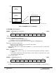
Table 15 768-Byte EEPROM Block Protection
Bit Name Block Protected Block Size
BPROT4 $0D00 to $0DFF 256 Bytes
BPROT3 $0E00 to $0EFF 256 Bytes
BPROT2 $0F00 to $0F7F 128 Bytes
BPROT1 $0F80 to $0FBF 64 Bytes
BPROT0 $0FC0 to $0FFF 64 Bytes
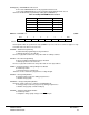
EETST — EEPROM Test $00F2
Bit 7 6 5 4 3 2 1 Bit 0
EEODD EEVEN MARG EECPD EECPRD 0 EECPM 0
RESET: 0 0 0 0 0 0 0 0