
Operating instructions


2-10 Overview
MB*/* Installation and Operation Manual
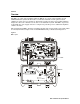
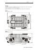
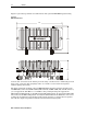
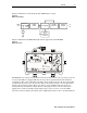
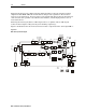
Following the Bode board, a JXP pad facility adjusts the RF level into the interstage hybrid
amplifier and the MDR-*MB/*/II controls flatness and provides equalization. Because these
losses are located interstage, the noise figure is only significantly impacted by the insertion loss
of the forward cable equalizer or broadband cable simulator, and the input pad if its value is
increased from zero.
Following the interstage hybrid is a JXP-*B pad socket (or a splitter and two JXP-*B pad
sockets for dual output) leading into the power-doubling output stage.
Figure 2-12 illustrates the interconnection between these components in the dual-output MB*/*:
Figure 2-12
MB*/* dual output block diagram
Input
port 1
Port
2
Port
4
Port
3
DC SP
JMP
RF/
AC
RF/
AC
RF
RF
AC
AC
(Status
Monitor
Output)
Manual Auto
H
L
**
** ** ** **
**
**
**
JXP-B
JXP-B
JXP-B
JXP-B
MDRBODE
** **
**
**** **
** **
**
SRE JXP-BTHERM
** **
JXPICS
JXPICS
Fuse
**
**
Fuse
Fuse
Fuse
Power
supply
Plug-in
module
24 Vdc
****
JXP-B
ADU/
TDU
RF/AC
RF
AC
DC/
SP/
JMP
RF/
AC
RF
AC
To status
monitor
**
H
L
-1.0 dB
-1.0 dB
-1.0 dB
+25.0 dB E-GaAs
+23.0 dB Silicon
Fltn.
Cntrl.
-4.0 dB -6.5 dB -1.0 dB +19 dB -4.0 dB
-4.0 dB
H
L
**
-1.0 dB
-1.0 dB
-1.7 dB F
-1.0 dB R
-20 dB
TP
-20 dB
TP
-20 dB
TP
-20 dB
TP
-20 dB
TP
-20 dB
TP
-1.7 dB F
-1.0 dB R
-2.0 dB F
-1.0 dB
-1.0 dB
SFE
or
SCS
PD
PD
PP
PP
-1.0 dB R
-0.4 dB -0.5 dB
Status
Monitor
Input
**
JXP-B
-16 dB+25.0 dB L
+30.0 dB H
-0.3 dB -4.0 dB
-4.0 dB
-0.4 dB
-0.4 dB
-0.4 dB
+18.0 dB E-GaAs
+20.5 dB Silicon
+18.0 dB E-GaAs
+20.5 dB Hi Gain
JXP-B
JXP-B
OnBrd
Atten
LPF
-0.4 dB
Surge
protector
Surge
protector