
Typewriter User Manual


MOTOROLA MC68340 USER’S MANUAL 4- 13
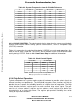
Table 4-2. System Frequencies from 32.768-kHz Reference
Y W = 0; X = 0 W = 0; X = 1 W = 1; X = 0 W = 1; X = 1
000000 131 262 524 1049
000101 786 1573 3146 6291
001010 1442 2884 5767 11534
001111 2097 4194 8389 16777
010100 2753 5505 11010 22020
011001 3408 6816 13631 –
011111 4194 8389 16777 –
100011 4719 9437 18874 –
101000 5374 10748 21496 –
101101 6029 12059 24117 –
110010 6685 13369 – –
110111 7340 14680 – –
111100 7995 15991 – –
111111 8389 16777 – –
NOTE: System frequencies are in kHz.
4.2.3.3 CLOCK CONTROL. The clock control circuits determine the source used for both
internal and external clocks during special circumstances, such as low-power stop
(LPSTOP) execution.
Table 4-3 summarizes the clock activity during LPSTOP in crystal mode operation. Any
clock in the off state is held low. The STEXT and STSIM bits in the SYNCR control clock
activity during LPSTOP. Refer to 4.2.6 Low-Power Stop for additional information.
Table 4-3. Clock Control Signals
Control Bits Clock Outputs
STSIM STEXT SIMCLK CLKOUT
0 0 EXTAL Off
0 1 EXTAL EXTAL
1 0 VCO Off
1 1 VCO VCO
NOTE: SIMCLK runs the periodic interrupt RESET and
IRQ≈ pin synchronizers in LPSTOP mode.
4.2.4 Chip Select Operation
Typical microprocessor systems require external hardware to provide select signals to
external memory and peripherals. The MC68340 integrates these functions on chip to
provide the cost, speed, and reliability benefits of a higher level of integration. The chip
select function contains register pairs for each external chip select signal. The pair
consists of a base address register and an address mask register that define the
characteristics of a single chip select. The register pair provides flexibility for a wide
variety of chip select functions.
Frees
cale Semiconductor,
I
Freescale Semiconductor, Inc.
For More Information On This Product,
Go to: www.freescale.com
nc...