
Typewriter User Manual


4- 34 MC68340 USER’S MANUAL MOTOROLA
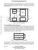
4.3.5.2 PORT A PIN ASSIGNMENT REGISTER 2 (PPARA2). PPARA2 selects between
an address and
IACK≈ function for the port A pins. Any set bit defines the corresponding
pin to be an
IACK≈ output pin. Any cleared bit defines the corresponding pin to be an
address bit as defined in the register diagram. Any set bits in PPARA1 override the
configuration set in PPARA2. Bit 0 has no function in this register because there is no
level 0 interrupt. This register can be read or written at any time.
PPARA2 $017
76543210
IACK7
(A31)
IACK6
(A30)
IACK5
(A29)
IACK4
(A28)
IACK3
(A27)
IACK2
(A26)
IACK1
(A25)
0
RESET:
00000000
Supervisor Only
The
IACK≈ signals are asserted if a bit in PPARA2 is set and the CPU32 services an
external interrupt at the corresponding level.
IACK≈ signals have the same timing as
address strobes.
NOTE:
Upon reset, port A is configured as an input port.
4.3.5.3 PORT A DATA DIRECTION REGISTER (DDRA). DDRA controls the direction of
the pin drivers when the pins are configured as I/O. Any set bit configures the
corresponding pin as an output. Any cleared bit configures the corresponding pin as an
input. This register affects only pins configured as discrete I/O. This register can be read
or written at any time.
DDRA $013
76543210
DD7 DD6 DD5 DD4 DD3 DD2 DD1 DD0
RESET:
00000000
Supervisor/User
4.3.5.4 PORT A DATA REGISTER (PORTA). PORTA affects only pins configured as
discrete I/O. A write to PORTA is stored in the internal data latch, and if any port A pin is
configured as an output, the value stored for that bit is driven on the pin. A read of PORTA
returns the value at the pin only if the pin is configured as discrete input. Otherwise, the
value read is the value stored in the internal data latch. This register can be read or written
at any time.
PORTA $011
76543210
P7 P6 P5 P4 P3 P2 P1 P0
RESET:
UUUUUUUU
Supervisor/User
Frees
cale Semiconductor,
I
Freescale Semiconductor, Inc.
For More Information On This Product,
Go to: www.freescale.com
nc...