
Typewriter User Manual


MOTOROLA MC68340 USER’S MANUAL 5- 99
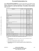
5.7.3.1 FETCH EFFECTIVE ADDRESS. The fetch EA table indicates the number of clock
periods needed for the processor to calculate and fetch the specified EA. The total
number of clock cycles is outside the parentheses. The numbers inside parentheses
(r/p/w) are included in the total clock cycle number. All timing data assumes two-clock
reads and writes.
Instruction Head Tail Cycles Notes
Dn
– – 0(0/0/0) –
An
– – 0(0/0/0) –
(An)
1 1 3(X/0/0) 1
(An)+
1 1 3(X/0/0) 1
−(An)
2 2 4(X/0/0) 1
(d
16
,An) or (d
16
,PC)
1 3 5(X/1/0) 1,3
(xxx).W
1 3 5(X/1/0) 1
(xxx).L
1 5 7(X/2/0) 1
#〈data〉.B
1 1 3(0/1/0) 1
#〈data〉.W
1 1 3(0/1/0) 1
#〈data〉.L
1 3 5(0/2/0) 1
(d
8
,An,Xn.Sz × Sc) or (d
8
,PC,Xn.Sz × Sc)
4 2 8(X/1/0) 1,2,3,4
(0) (All Suppressed)
2 2 6(X/1/0) 1,4
(d
16
)
1 3 7(X/2/0) 1,4
(d
32
)
1 5 9(X/3/0) 1,4
(An)
1 1 5(X/1/0) 1,2,4
(Xm.Sz × Sc)
4 2 8(X/1/0) 1,2,4
(An,Xm.Sz × Sc)
4 2 8(X/1/0) 1,2,3,4
(d
16
,An) or (d
16
,PC)
1 3 7(X/2/0) 1,3,4
(d
32
,An) or (d
32
,PC)
1 5 9(X/3/0) 1,3,4
(d
16
,An,Xm) or (d
16
,PC,Xm)
2 2 8(X/2/0) 1,3,4
(d
32
,An,Xm) or (d
32
,PC,Xm)
1 3 9(X/3/0) 1,3,4
(d
16
,An,Xm.Sz × Sc) or (d
16
,PC,Xm.Sz × Sc)
2 2 8(X/2/0) 1,2,3,4
(d
32
,An,Xm.Sz × Sc) or (d
32
,PC,Xm.Sz × Sc)
1 3 9(X/3/0) 1,2,3,4
X = There is one bus cycle for byte and word operands and two bus cycles for long-word operands.
For long-word bus cycles, add two clocks to the tail and to the number of cycles.
NOTES:
1. The read of the EA and replacement fetches overlap the head of the operation by the amount
specified in the tail.
2. Size and scale of the index register do not affect execution time.
3. The PC may be substituted for the base address register An.
4. When adjusting the prefetch time for slower buses, extra clocks may be subtracted from the
head until the head reaches zero, at which time additional clocks must be added to both the tail
and cycle counts.
Frees
cale Semiconductor,
I
Freescale Semiconductor, Inc.
For More Information On This Product,
Go to: www.freescale.com
nc...