
Typewriter User Manual


6- 8 MC68340 USER’S MANUAL MOTOROLA
.....
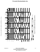
A31–A0
FC3–FC0
SIZ1–SIZ0
R/W
AS
DS
DSACKx
S0 S2 S4 S0 S2 S4 S0 S2 S4 S0
D15–D0
DREQx
DACKx
DONEx
(OUTPUT)
CPU CYCLEDMA READ
CPU CYCLE
NOTE:
1. Timing to generate more than one DMA request.
2. DACKx and DONEx (DMA control signals) are asserted in the source (read) DMA cycle.
3. DREQx must be asserted while DACKx is asserted and meet the setup and hold times for
more than one DMA transfer to be recognized.
DMA READ
CLKOUT
DONEx
(INPUT)
Figure 6-5. Single-Address Read Timing (External Burst)
Frees
cale Semiconductor,
I
Freescale Semiconductor, Inc.
For More Information On This Product,
Go to: www.freescale.com
nc...