
Typewriter User Manual


9- 2 MC68340 USER’S MANUAL MOTOROLA
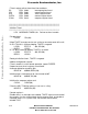
An overview of the MC68340 implementation of IEEE 1149.1 is shown in Figure 9-1. The
MC68340 implementation includes a 16-state controller, a 3-bit instruction register, and
two test registers (a 1-bit bypass register and a 132-bit boundary scan register). This
implementation includes a dedicated TAP consisting of the following signals:
TCK — a test clock input to synchronize the test logic
TMS — a test mode select input (with an internal pullup resistor) that is sampled on
the rising edge of TCK to sequence the TAP controller's state machine
TDI — a test data input (with an internal pullup resistor) that is sampled on the
rising edge of TCK.
TDO — a three-state test data output that is actively driven in the shift-IR and shift-
DR controller states. TDO changes on the falling edge of TCK.
3-BIT INSTRUCTION REGISTER
DECODER
TAP
CTLR
TMS
TCK
BOUNDARY SCAN REGISTER
BYPASS
TDI
M
U
X
M
U
X
TDO
TEST DATA REGISTERS
(133 BITS)
2
0
132
0
Figure 9-1. Test Access Port Block Diagram
9.2 TAP CONTROLLER
The TAP controller is responsible for interpreting the sequence of logical values on the
TMS signal. It is a synchronous state machine that controls the operation of the JTAG
logic. The state machine is shown in Figure 9-2; the value shown adjacent to each arc
represents the value of the TMS signal sampled on the rising edge of the TCK signal. For
a description of the TAP controller states, please refer to the IEEE 1149.1 document.
Frees
cale Semiconductor,
I
Freescale Semiconductor, Inc.
For More Information On This Product,
Go to: www.freescale.com
nc...