
Typewriter User Manual


MOTOROLA MC68340 USER’S MANUAL 9- 9
1
MUX
1
G1
1
MUX
1
G1
OUTPUT
FRO
M
SYSTEM
LOGI
C
FROM LAST
CELL
1D
C1
CLOCK DR
1D
C1
UPDATE DR
TO NEXT
CELL
TO OUTPUT
DRIVER
1 – EXTEST
0 – OTHERWISE
SHIFT DR
1
MUX
1
G1
FROM OUTPUT
ENABLE
FROM PIN
Figure 9-7. Bidirectional Data Cell (IO.Cell)
IO.CTL0
OR
IO.CTL1
IO.CELL
EN
FROM LAST CELL
OUTPUT
DAT
A
INPUT
DATA
OUTPUT
ENABL
E
I/O
PIN
TO NEXT CELL
TO NEXT
BIDIRECTIONAL
PIN
*
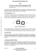
NOTE: More than one lO.Cell could be serially connected and controlled by a single IO.Ctlx cell.
Figure 9-8. General Arrangement for Bidirectional Pins
9.4 INSTRUCTION REGISTER
The MC68340 IEEE 1149.1 implementation includes the three mandatory public
instructions (EXTEST, SAMPLE/PRELOAD, and BYPASS), but does not support any of
the optional public instructions defined by IEEE 1149.1. One additional public instruction
(HI-Z) provides the capability for disabling all device output drivers. The MC68340
Frees
cale Semiconductor,
I
Freescale Semiconductor, Inc.
For More Information On This Product,
Go to: www.freescale.com
nc...