
Typewriter User Manual


MOTOROLA MC68340 USER’S MANUAL 10-3
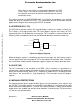
MC68340
XFC
V
CCSYN
0.1 F
1
NOTE 1: Must be a low-leakage capacitor.
V
CCSYN
0.1 F
µµ
0.01 F
µ
Figure 10-4. XFC and V
CCSYN
Capacitor Connections
10.1.2 Reset Circuitry
Because it is optional, reset circuitry is not shown in Figure 10-1. The MC68340 holds
itself in reset after power-up and asserts
RESET to the rest of the system. If an external
reset pushbutton switch is desired, an external reset circuit is easily constructed by using
open-collector cross-coupled NAND gates to debounce the output from the switch.
10.1.3 SRAM Interface
The SRAM interface is very simple when the programmable chip selects are used.
External circuitry to decode address information and circuitry to return data and size
acknowledge (
DSACK≈) is not required. However, external ICs are required to provide
write enables for the high and low bytes of data.
MCM6206-35
MCM6206-35
R/W
CE
E
R/W
CE
E
D7-D0
D15-D8
A15-A1
R/W
SIZ0
CS
D15-D0
MC68340
UWE
.
.
.
.
.
.
.
.
.
.
.
.
.
.
.
.
.
.
.
.
.
.
.
.
AS
LWE
A0
Figure 10-5. SRAM Interface
The SRAM interface shown in Figure 10-5 is a two-clock interface at 16.78-MHz operating
frequency. The MCM6206C-35 memories provide an access time of 15 ns when the chip
enable (
E) input is low. If buffers are required to reduce signal loading or if slower and less
expensive memories are desired, a three-clock cycle can be used. In the circuit shown in
Figure 10-5, additional memories can be used provided the MC68340 specification for
Frees
cale Semiconductor,
I
Freescale Semiconductor, Inc.
For More Information On This Product,
Go to: www.freescale.com
nc...