
Typewriter User Manual
11/2/95 SECTION 1: OVERVIEW UM Rev 1
MOTOROLA MC68340 USER'S MANUAL iii
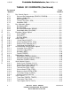
TABLE OF CONTENTS
Paragraph Page
Number Title Number
Section 1
Device Overview
1.1 M68300 Family.................................................................................................. 1-2
1.1.1 Organization.................................................................................................. 1-3
1.1.2 Advantages.................................................................................................... 1-3
1.2 Central Processor Unit..................................................................................... 1-3
1.2.1 CPU32............................................................................................................ 1-4
1.2.2 Background Debug Mode........................................................................... 1-4
1.3 On-Chip Peripherals ........................................................................................ 1-5
1.3.1 System Integration Module......................................................................... 1-5
1.3.1.1 External Bus Interface.............................................................................. 1-5
1.3.1.2 System Configuration and Protection................................................... 1-6
1.3.1.3 Clock Synthesizer..................................................................................... 1-6
1.3.1.4 Chip Select and Wait State Generation............................................... 1-6
1.3.1.5 Interrupt Handling..................................................................................... 1-6
1.3.1.6 Discrete I/O Pins........................................................................................ 1-6
1.3.1.7 IEEE 1149.1 Test Access Port................................................................ 1-7
1.3.2 Direct Memory Access Module................................................................... 1-7
1.3.3 Serial Module................................................................................................ 1-7
1.3.4 Timer Modules............................................................................................... 1-8
1.4 Power Consumption Management................................................................ 1-8
1.5 Physical.............................................................................................................. 1-9
1.6 Compact Disc-Interactive................................................................................ 1-9
1.7 More Information............................................................................................... 1-10
Section 2
Signal Descriptions
2.1 Signal Index....................................................................................................... 2-2
2.2 Address Bus....................................................................................................... 2-4
2.2.1 Address Bus (A23–A0) ................................................................................ 2-4
2.2.2 Address Bus (A31–A24).............................................................................. 2-4
2.3 Data Bus (D15–D0).......................................................................................... 2-4
2.4 Function Codes (FC3–FC0)............................................................................ 2-5
2.5 Chip Selects (
CS3–CS0) ................................................................................ 2-5
2.6 Interrupt Request Level (
IRQ7, IRQ6, IRQ5, IRQ3) ................................... 2-6
Frees
cale Semiconductor,
I
Freescale Semiconductor, Inc.
For More Information On This Product,
Go to: www.freescale.com
nc...