
Typewriter User Manual
11/2/95 SECTION 1: OVERVIEW UM Rev.1.0
iv MC68340 USER'S MANUAL MOTOROLA
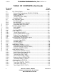
TABLE OF CONTENTS (Continued)
Paragraph Page
Number Title Number
2.7 Bus Control Signals ......................................................................................... 2-6
2.7.1 Data and Size Acknowledge (
DSACK1, DSACK0)................................ 2-6
2.7.2 Address Strobe (
AS).................................................................................... 2-6
2.7.3 Data Strobe (
DS)........................................................................................... 2-7
2.7.4 Transfer Size (SIZ1, SIZ0) .......................................................................... 2-7
2.7.5 Read/Write (R/
W)........................................................................................... 2-7
2.8 Bus Arbitration Signals.................................................................................... 2-7
2.8.1 Bus Request (
BR).......................................................................................... 2-7
2.8.2 Bus Grant (
BG)............................................................................................... 2-7
2.8.3 Bus Grant Acknowledge (
BGACK)............................................................. 2-7
2.8.4 Read-Modify-Write Cycle (
RMC)................................................................. 2-8
2.9 Exception Control Signals.............................................................................. 2-8
2.9.1 Reset (
RESET)............................................................................................... 2-8
2.9.2 Halt (
HALT).................................................................................................... 2-8
2.9.3 Bus Error (
BERR)........................................................................................... 2-8
2.10 Clock Signals.................................................................................................... 2-8
2.10.1 System Clock (CLKOUT)............................................................................ 2-8
2.10.2 Crystal Oscillator (EXTAL, XTAL)............................................................... 2-9
2.10.3 External Filter Capacitor (XFC) .................................................................. 2-9
2.10.4 Clock Mode Select (MODCK)..................................................................... 2-9
2.11 Instrumentation and Emulation Signals ....................................................... 2-9
2.11.1 Instruction Fetch (
IFETCH).......................................................................... 2-9
2.11.2 Instruction Pipe (
IPIPE)............................................................................... 2-9
2.11.3 Breakpoint (
BKPT)........................................................................................ 2-10
2.11.4 Freeze (FREEZE).......................................................................................... 2-10
2.12 DMA Module Signals....................................................................................... 2-10
2.12.1 DMA Request (
DREQ2, DREQ1)................................................................. 2-10
2.12.2 DMA Acknowledge (
DACK2, DACK1)...................................................... 2-10
2.12.3 DMA Done (
DONE2, DONE1)...................................................................... 2-10
2.13 Serial Module Signals..................................................................................... 2-11
2.13.1 Serial Crystal Oscillator (X2, X1) ............................................................... 2-11
2.13.2 Serial External Clock Input (SCLK)........................................................... 2-11
2.13.3 Receive Data (RxDA, RxDB)....................................................................... 2-11
2.13.4 Transmit Data (TxDA, TxDB)....................................................................... 2-11
2.13.5 Clear to Send (
CTSA, CTSB)..................................................................... 2-11
2.13.6 Request to Send (
RTSA, RTSB)................................................................ 2-11
2.13.7 Transmitter Ready (
T≈RDYA)..................................................................... 2-11
2.13.8 Receiver Ready (
R≈RDYA) ......................................................................... 2-12
2.14 Timer Signals.................................................................................................... 2-12
2.14.1 Timer Gate (
TGATE2, TGATE1)................................................................ 2-12
2.14.2 Timer Input (TIN2, TIN1) .............................................................................. 2-12
2.14.3 Timer Output (TOUT2, TOUT1)................................................................... 2-12
Frees
cale Semiconductor,
I
Freescale Semiconductor, Inc.
For More Information On This Product,
Go to: www.freescale.com
nc...