
Typewriter User Manual


3- 2 MC68340 USER’S MANUAL MOTOROLA
the sample window. If an input makes a transition during the window time period, the level
recognized by the MC68340 is not predictable; however, the MC68340 always resolves
the latched level to either a logic high or low before using it. In addition to meeting input
setup and hold times for deterministic operation, all input signals must obey the protocols
described in this section.
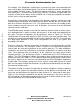
SAMPLE WINDOW
t
su
t
h
CLKOUT
EXT
Figure 3-1. Input Sample Window
NOTE
The terms
assert
and
negate
are used throughout this section
to avoid confusion when dealing with a mixture of active-low
and active-high signals. The term
assert
or
assertion
indicates
that a signal is active or true independent of the level
represented by a high or low voltage. The term
negate
or
negation
indicates that a signal is inactive or false.
3.1.1 Bus Control Signals
The MC68340 initiates a bus cycle by driving the A31–A0, SIZx, FCx, and R/W outputs. At
the beginning of a bus cycle, SIZ1 and SIZ0 are driven with FC3–FC0. SIZ1 and SIZ0
indicate the number of bytes remaining to be transferred during an operand cycle
(consisting of one or more bus cycles). Table 3-1 lists the encoding of the SIZx signal.
These signals are valid while
AS is asserted. The R/W signal determines the direction of
the transfer during a bus cycle. Driven at the beginning of a bus cycle, R/
W is valid while
AS is asserted. R/W only transitions when a write cycle is preceded by a read cycle or
vice versa. The signal may remain low for consecutive write cycles. The
RMC signal is
asserted at the beginning of the first bus cycle of a read-modify-write operation and
remains asserted until completion of the final bus cycle of the operation.
Frees
cale Semiconductor,
I
Freescale Semiconductor, Inc.
For More Information On This Product,
Go to: www.freescale.com
nc...