
Typewriter User Manual


MOTOROLA MC68340 USER’S MANUAL 3- 19
State 4—The MC68340 issues no new control signals during S4.
State 5—The MC68340 negates
AS and DS during S5. It holds the address and data valid
during S5 to provide address hold time for memory systems. R/
W, SIZ1/SIZ0, and FC3–
FC0 also remain valid throughout S5. The external device must keep
DSACK≈ asserted
until it detects the negation of
AS or DS (whichever it detects first). The device must
negate
DSACK≈ within approximately one clock period after sensing the negation of AS
or DS. DSACK≈ signals that remain asserted beyond this limit may be prematurely
detected for the next bus cycle.
3.3.3 Read-Modify-Write Cycle
The read-modify-write cycle performs a read, conditionally modifies the data in the
arithmetic logic unit, and may write the data out to memory. In the MC68340, this
operation is indivisible, providing semaphore capabilities for multiprocessor systems.
During the entire read-modify-write sequence, the MC68340 asserts
RMC to indicate that
an indivisible operation is occurring. The MC68340 does not issue a
BG signal in response
to a
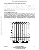
BR signal during this operation. Figure 3-9 is an example of a functional timing
diagram of a read-modify-write instruction specified in terms of clock periods.
CLK
A31–A30
FC3–FC0
S0 S2 S4 S2 S4 S0
S0
R/W
SIZ1–SIZ0
AS
DS
DSACKx
D15–D0
READ
WRITE
INDIVISIBLE
CYCLE
RMC
OUT
Figure 3-9. Read-Modify-Write Cycle Timing
Frees
cale Semiconductor,
I
Freescale Semiconductor, Inc.
For More Information On This Product,
Go to: www.freescale.com
nc...