
Typewriter User Manual


MOTOROLA MC68340 USER’S MANUAL 3- 21
proceeding to S4 and S5. To ensure that wait states are inserted, both DSACK1 and
DSACK0 must remain negated throughout the asynchronous input setup and hold times
around the end of S2. If wait states are added, the MC68340 continues to sample
DSACK≈ on the falling edges of the clock until one is recognized. The selected device
uses R/
W, DS, SIZ1/SIZ0, and A0 to latch data from the appropriate section(s) of D15–D8
and D7–D0. SIZ1/SIZ0 and A0 select the data bus sections. If it has not already done so,
the device asserts
DSACK≈ when it has successfully stored the data.
State 4—The MC68340 issues no new control signals during S4.
State 5—The MC68340 negates
AS and DS during S5. It holds the address and data valid
during S5 to provide address hold time for memory systems. R/
W and FC3–FC0 also
remain valid throughout S5. If more than one write cycle is required, states S0–S5 are
repeated for each write cycle. The external device keeps
DSACK≈ asserted until it detects
the negation of
AS or DS (whichever it detects first). The device must remove its data and
negate
DSACK≈ within approximately one clock period after sensing the negation of AS
or DS.
3.4 CPU SPACE CYCLES
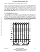
FC3–FC0 select user and supervisor program and data areas. The area selected by FC3–
FC0 = $7 is classified as the CPU space. The breakpoint acknowledge, LPSTOP
broadcast, module base address register access, and interrupt acknowledge cycles
described in the following paragraphs use CPU space. The CPU space type, which is
encoded on A19–A16 during a CPU space operation, indicates the function that the
MC68340 is performing. On the MC68340, four of the encodings are implemented as
shown in Figure 3-10. All unused values are reserved by Motorola for additional CPU
space types.
0000000000000000000 T0BKPT#
19 16
CPU SPACE CYCLES
FUNCTION
CODE
BREAKPOINT
ACKNOWLEDGE
0
0
00000
111111111111111110
19 16 0
ADDRESS BUS
1111
1
11111111111 1
LEVEL
19 16
0
CPU SPACE
TYPE FIELD
000000111111111100000000
19
16
0
111
0
LOW-POWER
STOP BROADCAST
111
0
INTERRUPT
ACKNOWLEDGE
111
0
11 1
0
MODULE BASE
ADDRESS
REGISTER ACCESS
0
0
3
3
3
3
0
0
00000000
31
31
111111111111
00000000
00000000
31
31
Figure 3-10. CPU Space Address Encoding
Frees
cale Semiconductor,
I
Freescale Semiconductor, Inc.
For More Information On This Product,
Go to: www.freescale.com
nc...