
Typewriter User Manual


3- 46 MC68340 USER’S MANUAL MOTOROLA
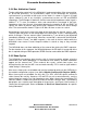
State 0—During state 0, the A31–A0 and FCx become valid, R/W is driven to indicate a
show read or write cycle, and the SIZx pins indicate the number of bytes to transfer.
During a read, the addressed peripheral is driving the data bus, and the user must take
care to avoid bus conflicts.
State 41—One-half clock cycle later,
DS (rather than AS) is asserted to indicate that
address information is valid.
State 42—No action occurs in state 42. The bus controller remains in state 42 (wait states
will be inserted) until the internal read cycle is complete.
State 43—When
DS is negated, show data is valid on the next falling edge of the system
clock. The external data bus drivers are enabled so that data becomes valid on the
external bus as soon as it is available on the internal bus.
State 0—The A31–A0, FCx, R/
W, and SIZx pins change to begin the next cycle. Data
from the preceding cycle is valid through state 0.
A31–A0,
FC2–FC0,
SIZ1–SIZ0
CLKOUT
S0 S42 S1S41 S43 S2
S0
R/W
AS, CS
DS
D15–D0
BKPT
SHOW CYCLE
START OF EXTERNAL CYCLE
Figure 3-26. Show Cycle Timing Diagram
3.7 RESET OPERATION
The MC68340 has reset control logic to determine the cause of reset, synchronize it if
necessary, and assert the appropriate reset lines. The reset control logic can
independently drive three different lines:
1. EXTRST (external reset) drives the external
RESET pin.
2. CLKRST (clock reset) resets the clock module.
Frees
cale Semiconductor,
I
Freescale Semiconductor, Inc.
For More Information On This Product,
Go to: www.freescale.com
nc...