
User manual


Page 7
Document No. 80-15151 Issue 6 HEBER LTD
5.4.2.4 Clock Synthesiser Control
The SYNCR controls the operation of the main processor clock. The MC68340 is provided
with a 32.768KHz reference to which the main clock is phase locked. After reset, the main
clock defaults to 8.39MHz. The maximum clock frequency of the standard MC68340 is
16.77MHz.
5.4.2.5 System Protection
The SYPCR controls the bus monitors and software watchdog. Other safeguards in the
design give adequate protection against programme malfunction as a result of noise, etc.
The Software Watchdog feature is disabled, however, it could be used if required.
The Bus Monitor should be enabled and may be left set at its default of 64 clock cycles time-
out.
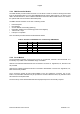
5.4.2.6 SIM40 Module Pin Allocations
Pins under the control of the SIM40 module are allocated as follows.
Table 1. Allocation of MC68340 Pins Controlled by SIM40 Module
NAME PIN I/O FUNCTION
PA0/A24- 123 O To I/O Expansion Connector P14, Pin b1, 3K3 pull-up &
RESET to Sound Channel #1, U8
PA1/A25/IACK1- 122 O To I/O Expansion Connector P14, Pin b2, 3K3 pull-up &
RESET to Sound Channel #2, U39
PA2/A26/IACK2- 121 O To I/O Expansion Connector P14, Pin b3, 3K3 pull-up &
Drive for Indicator LED LD2
PA3/A27/IACK3- 120 I To I/O Expansion Connector P14, Pin b4, 3K3 pull-up &
Push Button SW3 Input
PA4/A28/IACK4- 117 I/O To I/O Expansion Connector P14, Pin b5, 3K3 pull-up &
SCL line (I
2
C) to RTC, U40 and E
2
PROM, U37
PA5/A29/IACK5- 116 I/O To I/O Expansion Connector P14, Pin b6, 3K3 pull-up &
SDA line (I
2
C) to RTC, U40 and E
2
PROM, U37
PA6/A30/IACK6- 115 I/O Drives S1 pin on SFX Channel #2 (U39) 3K3 pull-up &
MPX Lamp Current Sense Input
PA7/A31/IACK7- 114 I/O Drives S2 pin on SFX Channel #2 (U39) 3K3 pull-up &
MPX Lamp Short Circuit Sense Input
PB0/MODCK 87 O Drive LOW to initiate hardware reset.
PB1/IRQ1-/CS1- 2 O CS1- Maps RAM
PB2/IRQ2-/CS2- 3 O CS2- Maps FPGA registers and I/O
PB3/IRQ3- 4 I Vmeter current sense input.
PB4/IRQ4-/CS3- 5 I/O To I/O Expansion Connector P14, Pin a3
PB5/IRQ5- 8 I/O To I/O Expansion Connector P14, Pin b15, 3K3 pull-up
PB6/IRQ6- 9 I/O To I/O Expansion Connector P14, Pin b16, 3K3 pull-up
PB7/IRQ7- 10 I IRQ7-/NMI input from Power Fail Detection Circuit
CS0-/AVEC- 1 O CS0- Maps ROM, both on-board U1/U2 and on Memory
Expansion Connector (via FPGA).