
Laptop User Manual


Preparation
http://www.motorola.com/computer/literature 1-7
1
The MCPN750A is factory tested and shipped with the configurations
described in the following sections. The MCPN750A’s required and
factory-installed debug monitor, PPCBug, operates with those factory
settings.
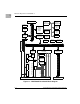
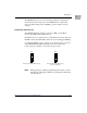
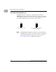
Flash Bank Selection (J7)
The MCPN750A baseboard has provision for 1MB of 16-bit Flash
memory and 4MB of linear Flash memory.
The Flash memory is organized in two banks, Bank A is 64 bits wide and
Bank B is 16 bits wide. Bank B contains the onboard debugger, PPCBug.
To enable Flash Bank A, place a jumper across header J7 pins 1 and 2. To
enable Flash Bank B (1MB of firmware located in sockets on the
baseboard), place a jumper across header J7 pins 2 and 3.
Note Placing a jumper on Flash programming header J9 has no affect.
The Flash programming for Bank A is permanently enabled with
onboard resistors.
3
2
1
3
2
1
Flash Bank A Enabled (4MB Soldered)
Flash Bank B Enabled (1MB, Sockets)
J7J7
(Factory Configuration)