
Development Board User's Manual

16
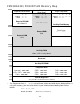
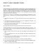
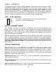
PRU PORT CONNECTOR
+5V
1 2
+5V
XPB6
3 4
XPB7
XPB4
5 6
XPB5
XPB2
7 8
XPB3
XPB0
9 10
XPB1
XPA6
11 12
XPA7
XPA4
13 14
XPA5
XPA2
15 16
XPA3
XPA0
17 18
XPA1
XPE6
19 20
XPE7
XPE4
21 22
XPE5
XPE2
23 24
XPE3
PE0
25 26
PE1
XPK4
27 28
XPK7
XPK2
29 30
XPK5
XPK0
31 32
XPK3
GND
33 34
XPK1
Note: PE0 and PE1 are the same signals as the
HC12 Port E.
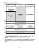
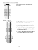
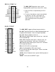
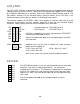
MCU_PORT 1
+5V
1 2
GND
PP0
3 4
PP1
PP2
5 6
PP3
PP4
7 8
PP5
PP6
9 10
PP7
PX0
11 12
PX1
PX2
13 14
PX3
PX4
15 16
PX5
PX6
17 18
PX7
PS6
19 20
PS7
PS4
21 22
PS5
PS2
23 24
PS3
PS0
25 26
PS1
PT0
27 28
PT1
PT2
29 30
PT3
PT4
31 32
PT5
PT6
33 34
PT7
PG/PJ0
35 36
PG/PJ1
PG/PJ2
37 38
PG/PJ3
PG/PJ4
39 40
PG/PJ5
PG/PJ6
41 42
PG/PJ7
PH6
43 44
PH7
PH4
45 46
PH5
PH2
47 48
PH3
PH0
49 50
PH1
The MCU_PORT1 provides access to the peripheral
features and I/O lines of the HC12. Note:
1) Not all I/O Ports are provided by all HC12 MCUs.
2) The PX0 - PX7 port is the CAN channel port and
additional I/O provided by the HC12 devices
associated with that port. Some devices designate
this port as PCAN, PIB, ect.
3) The PG/PJx ports provide either the HC12 port G
or HC12 port J depending on device installed.