
Processor Users Manual

4-32 MPC8260 PowerQUICC II UserÕs Manual MOTOROLA
Part II. ConÞguration and Reset
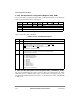
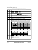
Table 4-12 describes SIUMCR Þelds.
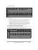
Table 4-12. SIUMCR Register Field Descriptions
Bits Name Description
0 BBD Bus busy disable.
0 ABB
/IRQ2 pin is ABB, DBB/IRQ3 pin is DBB
1 ABB/IRQ2 pin is IRQ2, DBB/IRQ3 pin is IRQ3
1 ESE External snoop enable. ConÞgures GBL/IRQ1
0 External snooping disabled. (GBL/IRQ1 pin is IRQ1.)
1 External snooping enabled. (GBL
/IRQ1 pin is GBL.)
2 PBSE Parity byte select enable.
0 Parity byte select is disabled. GPL4 output of UPM is available for memory control.
1 Parity byte select is enabled. GPL4 pin is used as parity byte select output from the MPC8260.
3 CDIS Core disable.
0 The MPC8260 core is enabled.
1 The MPC8260 core is disabled. MPC8260 functions as a slave device.
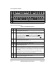
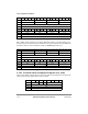
4Ð5 DPPC Data parity pins conÞguration. Note that the additional arbitration lines (EXT_BR2, EXT_BG2,
EXT_DBG2, EXT_BR3, EXT_BG3, and EXT_DBG3) are operational only when ACR[EARB] = 0.
Setting EARB (to choose external arbiter) combined with programming DPPC to 11 deactivates
these lines.
Pin
DPPC
00 01 10 11
DP(0)/RSR
V Ñ DP(0) RSRV EXT_BR2
DP(1)/IRQ1
IRQ1 DP(1) IRQ1 EXT_BG2
DP(2)/TLBISYNC
/IRQ2 IRQ2 DP(2) TLBISYNC EXT_DBG2
DP(3)/IRQ3
IRQ3 DP(3) CKSTP_OUT EXT_BR3
DP(4)/IRQ4
IRQ4 DP(4) CORE_SRESET EXT_BG3
DP(5)/TBEN
/IRQ5 IRQ5 DP(5) TBEN EXT_DBG3
DP(6)/CSE(0)/IRQ6
IRQ6 DP(6) CSE(0) IRQ6
DP(7)/CSE(1)/IRQ7
IRQ7 DP(7) CSE(1) IRQ7
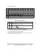
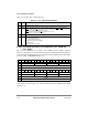
6Ð7 L2CPC L2 cache pins conÞguration.
Pin
Multiplexing
L2CPC = 00 L2CPC = 01 L2CPC = 10
CI/BADDR(29)/IRQ2 CI IRQ2 BADDR(29)
WT
/BADDR(30)/IRQ3 WT IRQ3 BADDR(30)
L2_HIT
/IRQ4 L2_HIT IRQ4 Ñ
CPU_BG
/BADDR(31)/IRQ5 CPU_BG IRQ5 BADDR(31)
8Ð9 LBPC Local bus pins conÞguration.
00 Local bus pins function as local bus
01 Reserved
10 Local bus pins function as core pins
11 Reserved