
Processor Users Manual

7-14 MPC8260 PowerQUICC II UserÕs Manual MOTOROLA
Part III. The Hardware Interface
7.2.7.1.1 Data Bus (D[0Ð63])ÑOutput
Following are the state meaning and timing comments for the D[0Ð63] output signals.
State Meaning Asserted/NegatedÑRepresents the state of data during a data write.
Byte lanes not selected for data transfer do not supply valid data.
MPC8260 duplicates data to enable valid data to be sent to different
port sizes.
Timing Comments Assertion/NegationÑInitial beat coincides with DBB
, for bursts,
transitions on the bus clock cycle following each assertion of T
A and,
for port size, transitions on the bus clock cycle following each
assertion of PSD
VAL.
High ImpedanceÑOccurs on the bus clock cycle after the Þnal
assertion of T
A, TEA, or certain ARTRY cases.
7.2.7.1.2 Data Bus (D[0Ð63])ÑInput
Following are the state meaning and timing comments for the D[0Ð63] input signals.
State Meaning Asserted/NegatedÑRepresents the state of data during a data read
transaction.
Timing Comments Assertion/NegationÑData must be valid on the same bus clock cycle
that T
A and/or PSDVAL is asserted.
7.2.7.2 Data Bus Parity (DP[0Ð7])
The eight data bus parity (DP[0Ð7]) signals both output and input signals.
7.2.7.2.1 Data Bus Parity (DP[0Ð7])ÑOutput
Following are the state meaning and timing comments for the DP[0Ð7] output signals.
State Meaning Asserted/NegatedÑRepresents odd parity for each of 8 bytes of data
write transactions. Odd parity means that an odd number of bits,
including the parity bit, are driven high. The signal assignments are
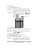
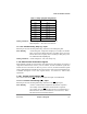
listed in Table 7-1.
Table 0-1. Data Bus Lane Assignments
Data Bus Signals Byte Lane
D0ÐD7 0
D8ÐD15 1
D16ÐD23 2
D24ÐD31 3
D32ÐD39 4
D40ÐD47 5
D48ÐD55 6
D56ÐD63 7