
Processor Users Manual

MOTOROLA Chapter 8. The 60x Bus 8-13
Part III. The Hardware Interface
8.4.3.2 Transfer Code Signals TC[0Ð2]
The transfer code signals, TC[0Ð2], provide supplemental information about the
corresponding address (mainly regarding the source of the transaction). Note that TCx
signals can be used with the TT[0Ð4] and TBST
to further deÞne the current transaction.
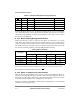
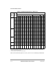
8.4.3.3 TBST and TSIZ[0Ð3] Signals and Size of Transfer
As shown in Table 8-4, the transfer size signals (TSIZ[0Ð3]) and the transfer burst signal
(TBST
) together indicate the size of the requested data transfer. These signals can be used
with address bits A[27Ð31] and the device port size to determine which portion of the data
bus contains valid data for a write transaction or which portion of the bus should contain
valid data for a read transaction.
The MPC8260 uses four double-word burst transactions for transferring cache blocks. For
these transactions, TSIZ[0Ð3] are encoded as 0b0010, and address bits A[27Ð28] determine
which double-word is sent Þrst.
The MPC8260 supports critical-word-Þrst burst transactions (double-word-aligned) from
the processor. The MPC8260 transfers the critical double word of data Þrst, followed by the
double words from increasing addresses, wrapping back to the beginning of the eight-word
block as required.
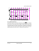
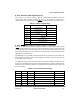
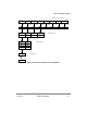
Table 8-3 Transfer Code Encoding
TC[0Ð2] Read Write
000 Core data transaction Any write
001 Core touch load Ñ
010 Core instruction fetch Ñ
011 Reserved Ñ
100 Reserved
101 Reserved
110 DMA function code 0
111 DMA function code 1
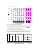
Table 8-4. Transfer Size Signal Encoding
TBST TSIZ[0Ð3] Transfer Size Comments Source
Negated 0 0 0 1 1 Byte Byte Core and DMA
Negated 0 0 1 0 2 Bytes Half-word Core and DMA
Negated 0 0 1 1 3 Bytes Ñ Core and DMA
Negated 0 1 0 0 4 Bytes Word Core and DMA
Negated 0 1 0 1 5 Bytes Extended 5 bytes SDMA (MPC8260 only)
Negated 0 1 1 0 6 Bytes Extended 6 bytes SDMA (MPC8260 only)