
Processor Users Manual

9-8 MPC8260 PowerQUICC II UserÕs Manual MOTOROLA
Part III. The Hardware Interface
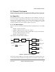
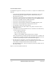
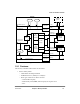
Figure 9-2. PLL Filtering Circuit
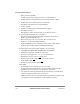
9.8 System Clock Control Register (SCCR)
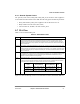
The system clock control register (SCCR), shown in Figure 9-3, is memory-mapped into
the MPC8260Õs internal space.
Table 9-4 describes SCCR Þelds.
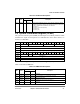
Bits 0 1 2 3 4 5 6 7 8 9 10 11 12 13 14 15
Field Ñ
Reset Ñ
R/W R/W
Addr 0x10C80
Bits 16 17 18 19 20 21 22 23 24 25 26 27 28 29 30 31
Field Ñ CLPD DFBRG
Reset Ñ 0 01
R/W R/W
Addr 0x10C82
Figure 9-3. System Clock Control Register (SCCR)
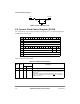
Table 9-4. SCCR Field Descriptions
Bits Name
Defaults
Description
POR Hard Reset
0Ð28 Ñ Reserved
29 CLPD 0 Unaffected CPM low power disable.
0 Default. CPM does not enter low power mode when the core enters low
power mode.
1 CPM and SIU enter low power mode when the core does. This may be
useful for debug tools that use the assertion of QREQ
as an indication of
breakpoint in the core.
10 W
VDD
0.1 µF
10 µF
VCCSYN