
Processor Users Manual

MOTOROLA Chapter 9. Clocks and Power Control 9-9
Part III. The Hardware Interface
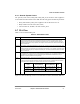
9.9 System Clock Mode Register (SCMR)
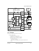
The system clock mode register (SCMR), shown in Figure 9-4, holds the parameters which
determine the output clock frequencies. To understand how these values interact, see
Section 9.4, ÒMain PLL.Ó
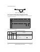
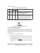
Table 9-5 describes SCMR Þelds.
30Ð31 DFBRG 01 Unaffected Division factor of BRGCLK from VCO_OUT (twice the CPM clock). DeÞnes
the BRGCLK frequency. Changing the value does not result in a loss of lock
condition. The BRGCLK is divided from the CPM clock.
00 Divide by 4
01 Divide by 16 (normal operation)
10 Divide by 64
11 Divide by 128
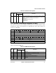
Bits 0 1 2 3 4 5 6 7 8 9 10 11 12 13 14 15
Field Ñ CORECNF
BUSDF CPMDF
Reset See Table 9-5
R/W R
Addr 0x10C88
Bits 16 17 18 19 20 21 22 23 24 25 26 27 28 29 30 31
Field Ñ
PLLDF PLLMF
Reset See Table 9-5
R/W R
Addr 0x10C8A
Figure 9-4. System Clock Mode Register (SCMR)
Table 9-5. SCMR Field Descriptions
Bits Name
Defaults
Description
POR Hard Reset
0Ð2 Ñ Ñ Ñ Reserved
3Ð7 CORECNF ConÞg pins Unaffected Core conÞguration. PLL conÞguration of the core.
8Ð11 BUSDF ConÞg pins Unaffected 60x bus division factor
12Ð15 CPMDF ConÞg pins Unaffected CPM division factor. This value is always 1.
16Ð18 Ñ Ñ Ñ Reserved
Table 9-4. SCCR Field Descriptions
Bits Name
Defaults
Description
POR Hard Reset